

Altium is one of the most popular design software worldwide. With its large component libraries and smart features, it outshines all its rival software. Year after year, the software keeps updating. Here we focus on the latest version, Altium 2017.
What is new
Altium is an all-in-one comprehensive software with a seamless exchange of design data. Be it schematic capture to PCB layout, or viewing MCAD constraints to providing a natural electronics workflow, Altium does it all. It adopts a much more efficient approach with user-defined enhancement.
Object-specific keep-outs
Designers face a lot of problems in routing and spacing between components. For instance, if high-voltage paths are not taken care of during design, these can cause damage to the circuit. Designers need to ensure that these have enough creepage and clearance distance from other tracks and components.

To explain, let’s consider the case of an LED driver manufacturing firm, where a designer designed a PCB without keeping in mind voltage differences across each point. During high-voltage test, the circuit failed with a high noise and copper peeling off.
Altium 2017 helps to overcome this issue by pointing out high-voltage areas or prohibited zones known as keep-out areas during designing. Besides, it has upgraded PCB routing.
Active routing
Whether the layout is single-layered, double-layered or multilayered, routing is now easy with Altium 2017’s active routing feature. From a single track to multiple tracks, all can be managed with a single click. Just select the nets and map-out the intended routing area. The tool not only saves time but also increases the efficiency greatly. Designers can produce multilayer boards with high-class routing.
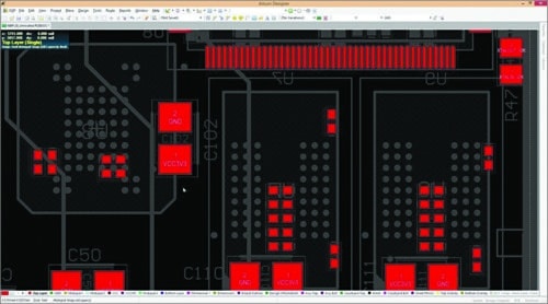
Fig. 1: Object-specific keep-outs (Image courtesy: https://i.ytimg.com)
Track glossing
The glossy feature lets designers clean up the routing segments and areas, giving the best finish to the end-product. It acts like an optimisation tool for quality and length of every net on the PCB, allowing automated alignment of routing paths.
Dynamic components/net selection
Designers can move, cut, paste or select any object in the layout easily. Earlier, during these functions, all the components used to get selected, whether required or not.
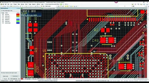
Fig. 2: Active routing (Image courtesy: https://i.ytimg.com)
Dynamic copper
This feature helps designers to maintain the copper volume around components, holes and vias as per the standard value of manufacturing. It easily combines copper shapes as per the layout requirement. Thus, judicial use of copper helps designers and manufacturers to save costs on copper usage.
Back drilling
Signal attenuation, crosstalks and reflections are the major drawbacks of any design layout. Even if the designer creates a design with perfection, disturbances caused due to vias, copper pads, tracks and component placement lead to improper results in PCBs designed for high-speed applications.
Backdrilling feature in Altium 2017 helps designers to automatically skip vias that may create issues during design in a particular segment of the PCB.

Fig. 3: Back drilling (Image courtesy: https://i.ytimg.com)
Auto-cross probing
Designers can quickly navigate between the PCB layout and the schematic in a single window, which helps them to net-list the components, nets and pins of components as well.
Last but not the least
With its new powerful features, Altium 2017 aims to reduce the stress on designers while giving a cost-effective solution to manufacturers. It provides a unified environment for schematic, PCB and documentation. Besides, it provides a PCB development platform featuring MCAD DNA with a single database providing both electrical and mechanical data. Above all, 3D vision gives a realistic view of multi-model support, component placement, clearance checking and rigid-flex design.
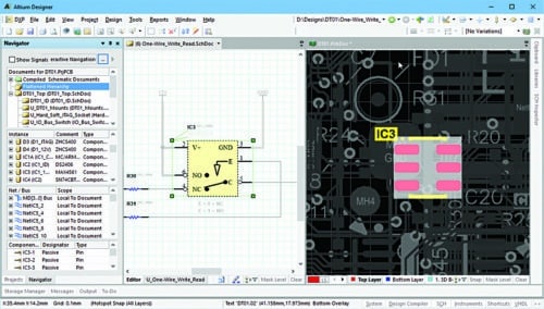
Fig. 4: Auto-cross probing (Image courtesy: www.altium.com)
Sourcing of components from the supplier is possible in one go using the Altium Library or vault. There is also a design history, which details differences between the existing and previous versions of Altium.
Download latest version of the software
