

Considering that every chip in the world and every transistor on the chip are tested, just imagine the amount of time and cost involved in testing millions of chips with billions of gates. semiconductor manufacturers are always looking for ways to reduce the test time and cost
SHWETA DHADIWAL BAID
Even if you use all the latest tools for your pre-silicon verification and develop the most accurate model near to the actual system, the biggest challenge is to get the first working silicon,” claims Rajamohan Varambally, director-technology R&D, STMicroelectronics, India.
The primary goal of post-silicon testing or validation is to ensure that the intent of your design is met. Varambally adds, “Making a chip for the first time will cost several million dollars. This is why whatever can be done with software is done beforehand so that the chances of coming up with correct silicon first time itself are high. However, software cannot simulate the entire working. Final testing has to be done on silicon.”
Silicon design and manufacturing processes have evolved over the years. Neeraj Rai, verification signoff manager, ASIC division, eInfochip, says, “The industry is dynamic and the methodology and languages have changed. The level of abstraction is a lot higher today. To support this, tool vendors and test equipment providers have developed more efficient and automated test systems.”

Post-silicon validation or testing has two aspects. Naresh Kumar, general manager, applications (EMG), Agilent Technologies, explains, “Once the first silicon is made, it is tested for functionality using discrete equipment or configured automated test equipment (ATE) before sending for mass production. Every chip produced is then tested using large testers.” In functional test, fault-finding or debugging is critical, while in production time-to-test is critical.
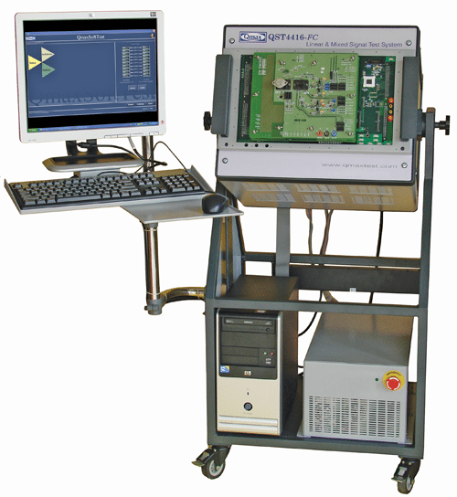
SoC: Need for embedded multi-functional tester
As every chip is designed for different purpose, the test parameters and process for functional test vary from chip to chip. Testing a chip for its functionality is basically providing a stimulus and measuring the response. There are advanced test systems like the ATEs which are configured to perform test on a particular chip.
“Once the designer provides specifications of the integrated circuit (IC), test programs are written to test its functionality. The program will feed in the inputs and measure the corresponding output to validate the functionality as per the specifications,” explains Veerappan V., co-founder and president-operations, Tessolve.
Rai adds “A test program written to test an analogue-to-digital converter (ADC) will be much different from the test program written for testing MP3 decoder chip.” It is very important to correctly program the ATE to do the functional testing.
There are analogue, digital and mixed test systems to test various parameters of the chips. The development of system-on-a-chip (SoC) demands testing of multiple functions simultaneously. The biggest challenge here is the development of multifunctional test programs. Embedded multifunctional test is of increasing importance in enabling SoC technology. There are software tools that help in test program conversion and enable smooth multifunctional tests.
Characterisation and reliability tests
Apart from testing for the actual functionality, the chips need to be tested in several different environments. Chips are tested for various domains like electrical validation, thermal characterisation, voltage and current graphs.
Electrical design validation helps to assess whether the given IC complies with a variety of different operating specifications, while reliability analysis helps to deduce the long-term reliability of the semiconductor and its suitability for intended applications.
Veerappan explains, “If a chip has a certain operating temperature, its performance is tested for varying temperature. Similarly, if the chip operates at 2 GHz, its operation is tested at 1.9 GHz and 2.1 GHz.” It’s like quality certification of the finished device before it goes for mass packaging.
Kumar says, “In addition to functional testing, DC and AC parametric testing is a big challenge, as with new processes the transistors need to be characterised and verified for their DC and AC characteristics. There are parametric tests which are performed to understand the semiconductor reliability, lifetime, device breakdown limits, etc. Typically, they involve current-voltage and capacitance-voltage characterisation of devices and then deriving reliability and other parameters from these tests.”
Biggest claim: chip is not working
The first working chip itself is a big challenge. Varambally says, “Another big challenge is to conclude that chip is faulty. One person cannot comment on that. So you need a team of experts to conclude that the chip is faulty or the design is faulty.”
Detecting a bug is not the only key thing in testing, pinpointing it in a large and complicated chip is also very important. “Several years ago, designing and testing were two independent processes. Today, a new process of concurrent or co-design and verification is used where the designer and test engineer work together to detect the fault at an early stage,” shares Neeraj Bhardwaj, systems hardware architect, Texas Instruments.
