

Symbol creation. No matter how accomplished the in-built symbol libraries are, you will always have to make new symbols for your designs. Do make some symbols yourself while evaluating a tool to see if it is really quick to make and include them in the existing libraries. Some tools have a very complicated procedure for making new symbols and including them in your design, which results in designers being reluctant to make new symbols and they try to work around the problem with the existing ones.
Hierarchical designs. This is a must. When the design gets complex, it is better to represent it as a hierarchical design. This makes the representation simple, traceable, and easy to navigate and review. In schematics with a lot of repetition, this feature can save you labour. For example, if you have 10 channels of some circuitry, you can build it once and replicate it using hierarchy. Second, when multiple persons are working on a project, it enforces clean boundaries. Because all high-level connectivity is via ports, there is no risk of accidental connectivity via off-page connectors. And yet, within each subsection of the design, you can still use off-page connection if you like. Also check the page limitation, if any, for multi-sheet designs.

ERC (electrical rule check). The ERC is used to test schematics for electrical errors such as unconnected inputs, shorted outputs, correct power and ground connections. When you are working on a schematic, there will be some human errors that can lead to tears at a later stage of development. This feature can catch such silly mistakes in time to save you from a lot of suffering.
Smart features. Smart features such as auto-number, replace, slot, etc, are highly useful. For example, if there are 20 resistors in your design and you name them one by one, it will take too much time. But if you can select them all and use the auto-number function, resistors get incremented reference numbers automatically. Such functions save time and reduce human error, so do look for them in any EDA tool you are reviewing.
Supported image formats. Often, you will have to publish your schematic, for which you need it in some image format such as EPS, JPEG, etc. Do check if the image format required by you is supported by the EDA.
Configurability. All EDAs are designed corresponding to standard needs but every organisation has unique requirements for an EDA. For example, one organisation might need a different colour-map for exported images or a BOM in a different format, and so on. Here, configuration comes into play. In proprietary tools, configuration access is only on the surface level and you can change only a very limited number of things. But several open source tools are completely configurable and you can change them to suit your needs. So if your organisation has such unique requirements which no proprietary software supports, then open source tools are what might help.
Exporting designs to the PCB tool
The EDA tool you select should support the complete design cycle. Once the schematic entry is done, it is simulated for verification. But as per past experiences, there is always some gap between the simulated and real result. Therefore prototyping is done and all the tests are performed on the physical sample. All electronic assemblies are done on the PCB board, so you have to make the PCB layout for your design. EDA tools should have the function that enables your design to be exported to the PCB design tool in an intuitive manner.
Some PCB tools even accept the netlist generated by other schematic capture tools for PCB layout. If you plan to work that way, check what netlist formats are accepted by the tool. Also, your organisation might outsource the PCB design work. So it is important that your schematic capture tool can generate a netlist compatible to other tools as well.
The PCB design tool
The PCB design tool is used to make the PCB layout of your design. The PCB is manufactured with this layout and components are mounted on it to build the prototype. PCB design is creative work, so the tool should be very efficient in handling repetitive cumbersome jobs and should be extremely user friendly. Also, this is one task in the design phase that requires a lot of concentration and has maximum chances of human error. So the tool should be able to automatically indicate the human errors.
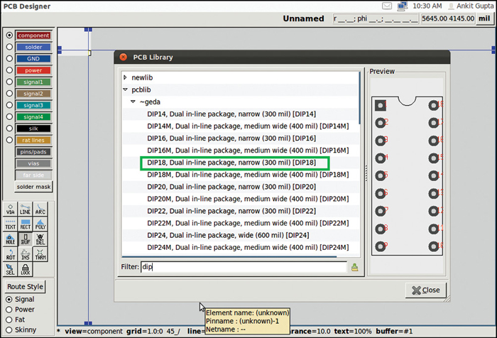
Similar to schematic capture tool, one of the key parameters to consider while selecting the PCB tool are the available in-built footprint library and quick footprint creation. The more complete the footprint library is, the less time you will spend making new footprints. Unlike symbols, footprints have to be created very precisely so that they match your components. The dimensions are very critical in this case, and making one takes more time than making a symbol.


