But as I have already explained, you will always have to make new footprints. So it is better that the process of making one is simple and quick. Some open source tools even support footprints created by other third-party tools (which are specifically designed to make footprints) and are very efficient and precise. The availability of such features is also a plus point while selecting an EDA tool.
Other features that should be available in the PCB design tool are:
Multi-layer design. Some PCB design tools support a limited number of layers. Here you should consider your future prospects also and look for a tool that can support the maximum number of layers. As the designs become complex, it becomes difficult to lay out a PCB design on a single layer in conformance with the design guidelines. You will need multi-layer functionality today or tomorrow, so it is best that you think about it in advance, rather than regret your choice at a later stage.

Smart functions. Similar to schematic capture, smart functions such as auto-placement, auto routing, etc, can speed up the work. If some design portions are not very critical, you can select the corresponding components and run ‘auto-placement’ to place the components together. In this way, you do not have to take components one by one and think too much about how to place them. After this, you can even auto-route them. Entire routing will be done all at once. This saves a lot of time. Though auto-routing and auto-placement algorithms are improving, it is still preferable to do it manually. But you can save some time using these features for non-critical portions.
Forward and backward annotation. With this feature, schematic and PCB files are logically interconnected through automatic forward and backward annotation. When you add a new part to a schematic, the part’s package is added to the PCB layout automatically and you do not have to import it again. When deleting a part from a schematic drawing, the part’s package is deleted from the PCB layout as well.
Similarly, when a part is deleted from the PCB layout file, the corresponding part will be deleted from the schematic as well. This is a very useful feature, so grab an EDA tool with this functionality.
DRC (design rule check). This is a very important feature that checks the design for various standard design guidelines automatically. The main objective of the DRC is to achieve a high overall yield and reliability for the design. While design rule checks do not ensure that the design will operate correctly, they are constructed to verify that the structure meets the process constraints for a given design type and process technology. So if your PCB design tool could have this feature, you can avoid a lot of process related mistakes automatically.
Exports/imports
Once the design is complete, you will create the manufacturing data. Carefully check if all standard exports like Gerber, netlist, BOM, etc, are available. Check this aspect for imports too.
Simulation
Simulation modelling allows designers and engineers to avoid repeatedly building multiple physical prototypes to analyse designs for new or existing parts. Before creating the physical prototype, users can virtually investigate many digital prototypes. Electronic circuit simulation uses mathematical models to replicate the behaviour of an actual electronic device or circuit. Simulation software allows for the modelling of circuit operations and is an invaluable analysis tool.
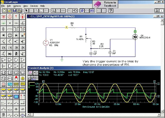
While there are mostly analogue electronics circuit simulators, popular simulators often include both analogue and digital simulation capabilities. This means that any simulation may contain components that are analogue, digital or a combination of both. An entire mixed signal analysis can be driven from one integrated schematic. So when you are selecting the EDA, simulation is a must in the tool chain. Look for a mixed signal simulation system.
Gerber viewer
The Gerber file format is used by printed circuit board industry software to describe the PCB image’s copper layers, solder mask, legend, drill holes, etc. The Gerber file format is the de facto industry standard for printed circuit board image transfer. You will generate these Gerber files when you want to send the data to the manufacturer. Also, often you will need to view the Gerber files to see the real view of your PCB design. Therefore the Gerber viewer is also a must in the tool chain.
Do consider all the points mentioned above for various sub-tools, prior to selecting the right EDA for your organisation. It would be ideal if you can make the right selection at the first instance to save money and the most precious resource—time.
The author is a technical editor at EFY