
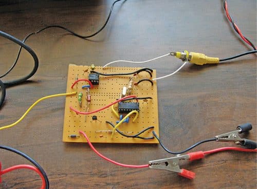
 A shortwave transmitter can be built with IC CD4049, which is used as an oscillator and a buffer amplifier. The transmitter can be crystal controlled to work at a frequency of 3MHz to 5MHz, which includes the ham radio bands of 3.5MHz to 3.7MHz and 3.89MHz to 3.9MHz. The author’s prototype is shown in Fig. 1.
Circuit and working
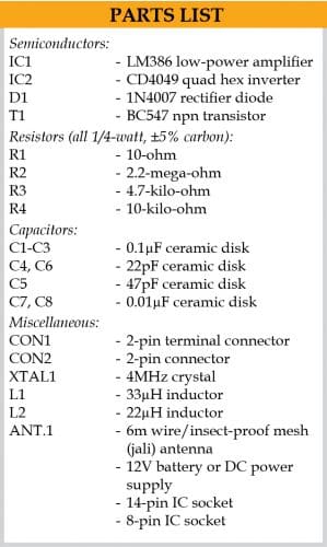
Circuit diagram of the shortwave transmitter using CD4049 and 4MHz crystal is shown in Fig. 2. It is built around LM386 (IC1), CD4049 (IC2), and transistor BC547 (T1).
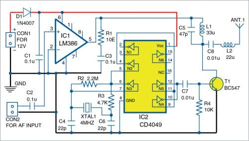
The IC CD4049 is a hex inverter that has six NOT or inverter gates of which only four are used in this circuit. The inverter gate between pin numbers 7 and 6 is used as a crystal controlled oscillator.
The output of the oscillator is given to the inverter gate between pin numbers 5 and 4, which is used as a buffer. The buffer’s output goes to two inverter gates between pin numbers 9 and 10 and 11 and 12, which are connected in parallel. The output of these gates goes to transistor T1, which is used as a modulator as well as class C amplifier.
This method of modulation is different from the modulation techniques used in transmitter circuits published earlier in EFY and is known as power conversion. If a class C device amplifying one frequency has its input power varied at second frequency, the output is modulated at the second frequency.

IC LM386 in the circuit is used as an audio frequency amplifier. The output of this amplifier goes to the collector of transistor T1 through the tuned circuit comprising capacitor C5 and inductor L1. It should be noted that the output of LM386 goes directly to the transistor and not through a capacitor, which is done when the IC is used as an audio frequency amplifier to drive a loudspeaker.
The DC voltage at collector of transistor should be half the power supply voltage under no-signal conditions. Thus, power to the transistor is varied at audio frequency and the amplitude modulated signal is obtained at its collector. The advantage of this method of modulation is that the output power can be easily increased by replacing the audio frequency amplifier with a higher power amplifier and replacing the transistor with one capable of handling more power.
The output of IC2 is a square wave and, according to Fourier analysis, a square wave consists of infinite series of sine waves of harmonics of the frequency of the square wave. The tuned circuit comprising capacitor C5 and inductor L1 is designed to select only the fundamental frequency; thus the output is a sine wave of 4MHz frequency with the values of C5 and L1 selected for the circuit.

In practice, L1 has some internal capacitance also, so C5 may be replaced by a preset of 47pF as the resonance may occur at a capacitance lower than 47pF with the preset tuned to get maximum output.
The output is coupled to the antenna by capacitor C8 and inductor L2. A wire of four to six metres length can be used as the antenna. Experimentally, the best results were obtained by using an insect-proof mesh (jali) in a window as antenna. The mesh was connected to the transmitter by using an ordinary 1.5 metre long wire. See Fig. 3.
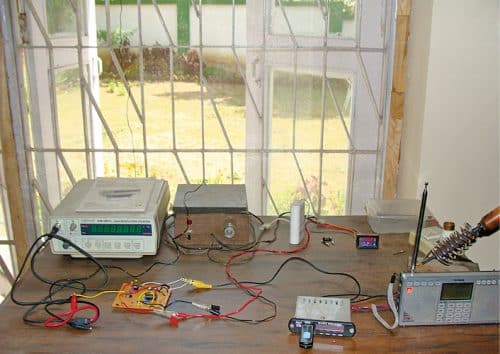
The audio source used for testing was a ‘Vire’ brand USB player. Excellent signals were received by using a Tecsun PL-390 radio receiver up to 500 metres away. If the audio source has a weak output, a 10µF capacitor can be connected between pins 1 and 8 of LM386. If the audio source has a strong output, it can be connected through a potentiometer to IC1.
The frequency of the oscillator can be changed by changing the crystal. An alternate method is to change L1 and C5 so that they form a tuned circuit that is tuned to first harmonic.
Construction and testing
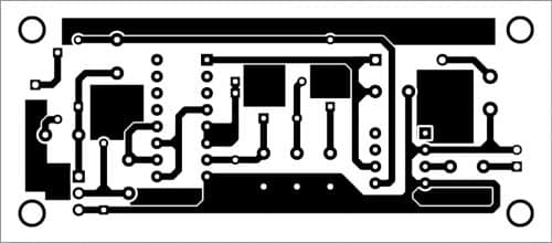
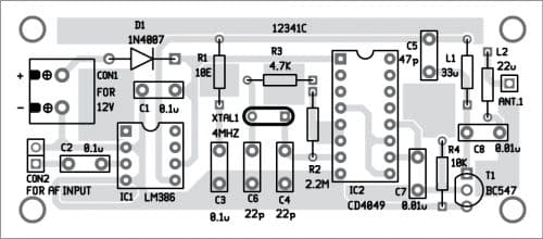
A PCB layout for the shortwave transmitter is shown in Fig. 4 and its components layout in Fig. 5.
Download PCB and Component Layout PDFs: click here
After wiring, connect 12V DC power supply across CON1. Connect audio output from your MP3 player, mobile phone, or laptop to the input of your transmitter across CON2 connector. You are now ready to transmit and receive the signals in a shortwave radio up to 500 metres away.
Pradeep Vasudeva is a member of The Indian Forest Service (1992 batch) presently posted in Jabalpur (MP). Electronics is his first love since adolescence and his areas of interest include RF circuits, ham radio, and audio projects.


