
This article describes a satellite finder that we can build ourselves to assist with aligning the satellite TV dish without having to take our receiver outside. We are proposing a signal strength measurement meter which will greatly help in optimizing the dish antenna alignment precisely, once after the satellite is located.
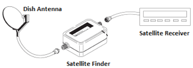
The utilization of satellite finder is shown in figure 1. The low noise block (LNB) down-converter used for satellite reception (digital or analogue) does not just receive a single channel; it receives the complete range from all transponders that are operating on a particular satellite. Together with the high gain a modern LNB feeds a lot of RF energy to the receiver when the dish is correctly aligned. Our digital satellite finder measures the amount of RF energy over a wide frequency range by summing the power from all transponders and producing Received Signal Strength Indicator (RSSI) output, by means of proportionate DC voltage for display.
Since most of the existing satellite finders are using analog scale only, and some of the satellite finders are partially digital (digital handling with analog display) and rarely available digital satellite finders are with high cost, Our innovative design explores latest technology for RF power measurement (RSSI) with digital read out, economically, and provides fruitful results to the dish TV installers.
RF Power Detector
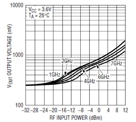
We are using the IC LTC 5508 from Linear Technology, for RF power measurement. The LTC5508 operates with input power levels from –32dBm to 12dBm.This IC is an RF power detector for RF applications operating in the 300MHz to 7GHz range. A temperature compensated Schottky diode peak detector and buffer amplifier are combined in a small SC70 package, to detect the RF power by means of dc output voltage. The detected voltage is buffered and supplied to the VOUT pin. Maximum power of RF signal produces peak output voltage as shown in the figure 3.
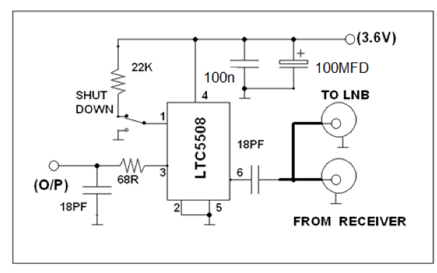
A logic low on the SHDN (pin1) disables the circuit and Logic high enables the circuit. This is done by a SPST switch (SW1) and resistor R2. The SHDN pin has an internal 150k pull down resistor to ensure that the part is in shutdown when no input is applied. This IC can be operated from the Supply Voltage, 2.7V to 6V. VCC is applied to the pin 4 and the capacitor C3 is used as bypass capacitor. A coupling capacitor C2 is used to connect to the RF signal source to the IC. The frequency range is 300MHz to 7GHz. This pin has an internal Schottky diode detector and a peak detector capacitor. The application circuit of LTC5508 is shown in figure 2.

LTC 5508 application
The LTC5508 RF detector integrates several functions to provide RF power detection over frequencies ranging from 300MHz to 7GHz. These functions include an internally compensated buffer amplifier, an RF Schottky diode peak detector and level shift amplifier to convert the RF input signal to DC, a delay circuit to avoid voltage transients at VOUT when coming out of shutdown and a gain compression circuit to extend the detector dynamic range. The buffer amplifier has a gain of two and is capable of driving a 2mA load. The buffer amplifier typically has an output voltage range of 0.25V to 1.75V.
The internal RF Schottky diode peak detector and level shift amplifier converts the RF input signal to a low frequency signal. The detector demonstrates excellent efficiency and linearity over a wide range of input power.
The LTC5508 can be used as a self-standing signal strength measuring receiver and depending on specific application needs, the RSSI output can be split into two branches, providing AC-coupled data output and DC-coupled, RSSI output for signal strength measurements and AGC. The following graph (Figure3) shows that proportionate DC output voltage for the relevant RF input signal. This is coupled to a digital volt meter through R1 & C1.
Power Supply
A built–in power supply is provided using the two consecutive voltage regulator ICs (LM1086-ADJ) as shown in figure 4. The supply voltages required, are obtained from the satellite receiver itself, using the same RF cable. The inductor 10mH (L1) acts as a RF choke to prevent RF signal from DC biasing to the satellite finder. The voltage regulators are designed using the IC LM1086 to provide 5V & 3.6V respectively. The 5V supply is used for digital display, and 3.6V supply is used for the RF power detector.

The LM1086 adjustable version develops a 1.25V reference voltage, (VREF), between the output terminal (pin2) and the adjust terminal (pin1), at 1.5 A of load current. Two resistors are required to set the output voltage of the adjustable output voltage version of the LM1086. Fixed output voltage versions integrate the adjust resistors. The Load Regulation is 0.1% (Typical) and the Line Regulation is 0.015%. The device component count is very minimal, employing two resistors as part of a voltage divider circuit and an output capacitor for load regulation. The voltage divider for this part is set based on the equations shown below; where R3/R5 is the upper feedback resistor R4/R6 is the lower feedback resistor.
VOUT = 1.25V (1+R6/R5) for 5V output
VOUT = 1.25V (1+R3/R4) for 3.6V output
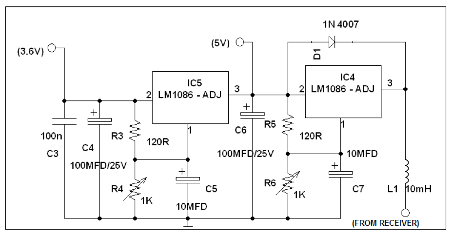
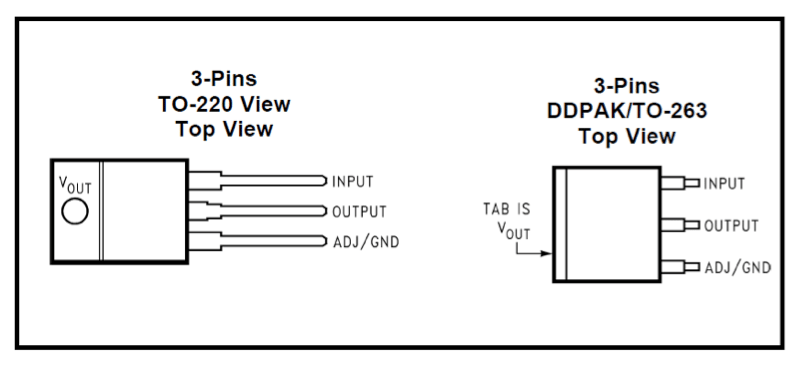
With a large output capacitor (≥100 μF), and with input instantaneously shorted to ground, the regulator could be damaged. In this case, an external diode (D1) is recommended between the output and input pins to protect the regulator. The capacitors C4 & C6 are used as output filters for both the regulators. The top view pin layout of IC LM1086 is shown below (figure5).
Digital Voltmeter
An accurate digital voltmeter using the IC L7107 from Intersil Corporation, is utilized for digital display. The application circuit is shown in figure6. The IC includes low power, 3.5 digits analog to digital converter, internal circuitry for seven segment decoders, display drivers, reference voltage source and a clock. The power dissipation is less than 10mW and the display stability is very high.
The working of this electronic circuit is very simple. The voltage to be measured is converted into a digital equivalent by the ADC inside the IC and then this digital equivalent is decoded to the seven segment format and then displayed. The ADC used in IC L7107 is dual slope type ADC. The process taking place inside our ADC can be stated as follows. For a fixed period of time the voltage to be measured is integrated to obtain a ramp at the output of the integrator. Then a known reference voltage of opposite polarity is applied to the input of the integrator and allowed to ramp until the output of integrator becomes zero.
Input voltage comparison & conversion
The time taken for the negative slope to reach zero is measured in terms of the IC’s clock cycle and it will be proportional to the voltage under measurement. In simple words, the input voltage is compared to an internal reference voltage and the result is converted in a digital format. The 14.2 mm (0.56 inch) LED seven segment displays are connected are available as common anode (DISP1 – DISP4). The resistor R13 and C13 are used to set the frequency of IC’s internal clock. Capacitor C12 neutralizes the fluctuations in the internal reference voltage and increases the stability of the display. A 0.1μF capacitor gives good results in most of the applications.
The resistor R10 controls the range of the voltmeter. Right most three displays are connected so that they can display all digits. The left most display is so connected that it can display only “1” and “-“.The pin5(representing the dot) is connected to ground only for the second display and its position needs to be changed when you change the range of the volt meter by altering R10. (R10 =1.2K gives 0-20V range, R10 =12K gives 0-200V range).
Digital voltmeter using IC L7107
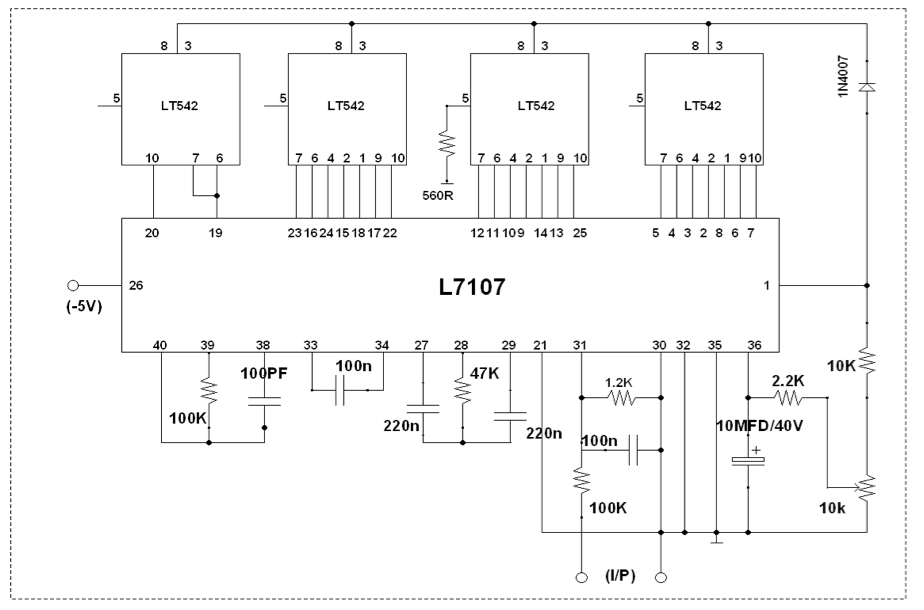
The analog input required to generate full scale output (2000 counts) is: VlN = 2VREF. Thus, for the 200mV and 2V scale, VREF should equal 100mV and 1V, respectively. This is done by the resistors R7,R8 & R9. The integrating resistor should be large enough to remain in this very linear region over the input voltage range. So we useR12 = 470K in our circuit. The integrating capacitor should be selected to give the maximum voltage swing and the nominal value is 0.22µF( C11). The size of the auto-zero capacitor (C10) has some influence on the noise of the system. On the 2V scale, a 0.047μF capacitor increases the speed of recovery from overload and is adequate for noise on this scale.
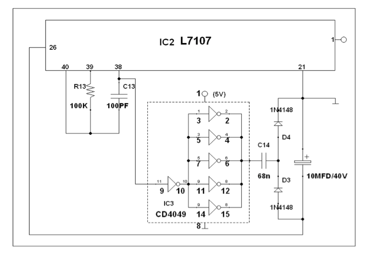
The display is 3 1/2 digits, which means that the maximum display 1999 course with a decimal point included if desired. Decimal point is connected through a resistor R14 to ground. It is also not necessary to use four displays; you can only use 3 to display 999 or range 100mV, 1V, 10V, 100V. The ICL7107 is designed to work from ±5V supplies. However, if a negative supply is not available, it can be generated from the clock output (pin 38 of IC2) with 2 diodes (D3&D4), 2 capacitors (C14 & C15), and an inexpensive IC CD4049 (IC3) as shown in the following figure7.
Note:
• Assemble the circuit on a good quality PCB.
• For calibration, power up the circuit and short the input terminals. Then adjust R8 so that the display reads 0V.
• The ICL7107 is a CMOS device and it is very sensitive to static electricity. So avoid touching the IC pins with your bare hands.
• The seven segment displays must by common anode type.
Operating Procedure
The installer can view a projection of the Azimuth and Elevation degrees simultaneously of incoming signals as well as measure and adjusting the antenna for the Azimuth and the Look Angle. The satellite signals can be visualized and any obstacles can be avoided.
The Site & Satellite Finder can be placed below the antenna dish the compass will give a correct reading for MAGNETIC as well as for NON-MAGNETIC satellite antennas. You need to know (at your location) the Azimuth adjusted for the declination (Magnetic north) and the Elevation Look Angle for each satellite you would like to receive signals from.
Disconnect the coax running from your receiver to the LNB (at the LNB end) then connect the signal meter to the LNB using a length of coax (between 1- 3 meters). The receiver can then also be plugged into the signal meter.
As the device can be interfaced symmetrically, you can connect the device either way round. Power from the receiver is needed, so leave your receiver powered on. But it is not necessary to set it to a specific channel.
Satellite finder circuit diagram
Point your dish in roughly the direction of the desired satellite, using either a compass or the shadow of the sun at a predetermined time. Use your favorite tracking program to determine the compass heading or the time when the sun reaches the same direction (azimuth) as the satellite. To increase the gain on the satellite signal, gently vary the azimuth and elevation of the satellite to maximize meter read-out. The digital display will read 2.5-2.8V to give better reception.
Be aware that only 5° off direction can mean that you won’t receive anything, or worse, you may have optimized on a neighboring satellite! Once you have found the best dish alignment, you can optimize the position of the LNB in the feed clamp. Try rotating the LNB slightly from the normal position and shifting it towards or away from the dish to obtain maximum read-out. Always check the reception on your receiver to verify that you have optimized on the correct satellite before fixing up your dish! If you are using a motorized polar mount, you can use the satellite meter at the receiver side too.
Experimental Circuit
(This is the circuit implemented and tested primarily (figure8), for which I have enclosed the prototype for your verification. The readings are observed with a Digital Multi Meter. The verified dish TV set up is AIRTEL)

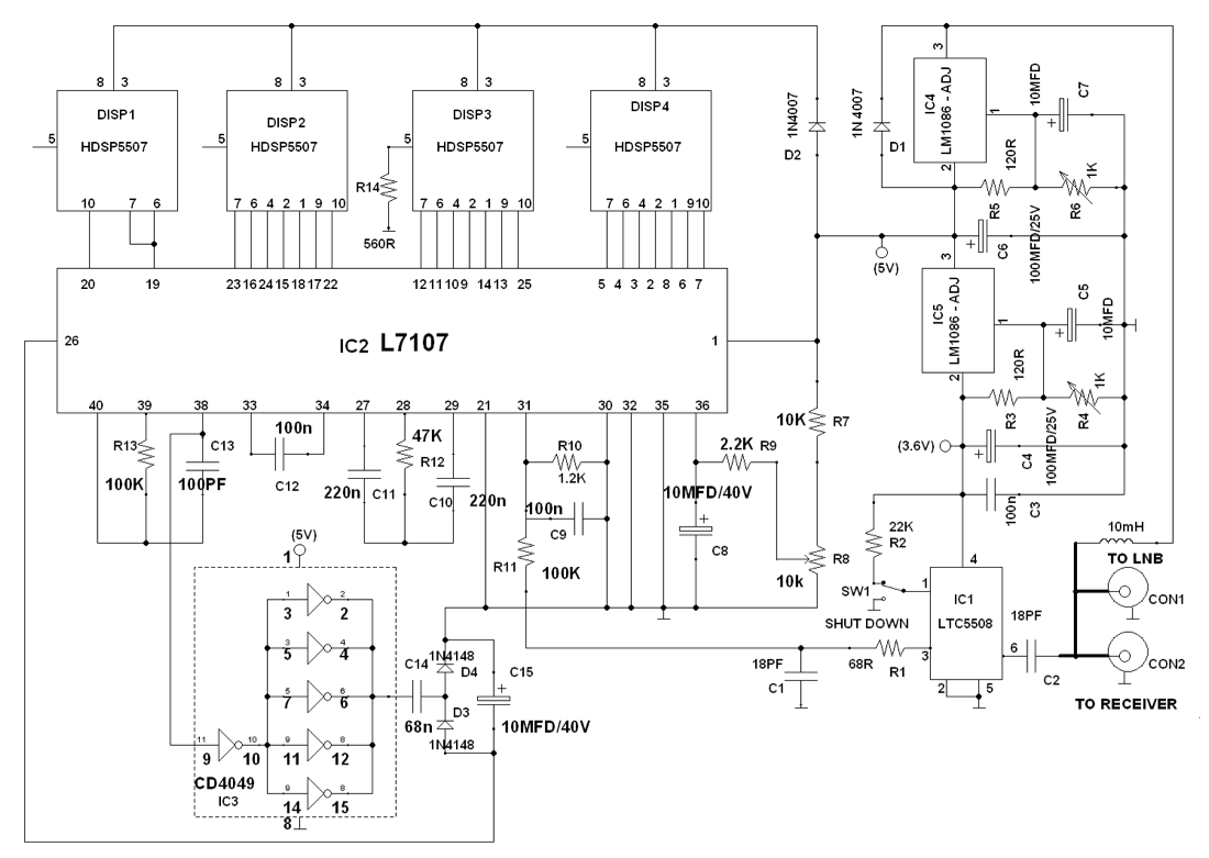
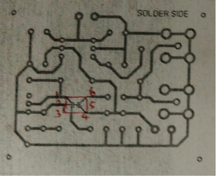
Although this design draws only a very small amount of RF from the LNB, it could degrade the performance of your system, so remove it after dish alignment has been completed. It is important that the wires shown thickly in the schematic diagram are kept as short as possible (less than 5 mm) as we are dealing with high frequencies here. Solder these parts directly to the back of the F-connector. Use a short length of coax to connect both F-connectors to each other inside the box. Finally, the completed unit must be housed in a metal box to prevent RF leaking out. The complete circuit diagram of the proposed digital Satellite finder is shown in the figure 8. The circuit made for experimental setup is shown in figure 9. The PCB layout and Component Layout for this experimental circuit is shown in figure 10 & 11 respectively.
We hope that this digital satellite finder will be a more useful tool for the installation and maintenance of dish TV connections.

(The layouts are not in the correct dimension)
Interested in circuits? Check out our circuits section for more interesting ideas.


good
its a very indepth electronic educational forum