
This article introduces a mixed logic design method that uses CNTFET technology combining the basic transmission gate logic, the pass transistor dual-value logic, and base CMOS logic. 14T and 15T configurations have been studied and analysed—14T for 2 to 4 decoder with low transistor count benefit and 15T for high performance in terms of power and delay using 15 transistors. The results are quite encouraging.
The very large scale integration (VLSI) technology has made it possible to fabricate millions of transistors on a single chip. As nanometer process innovations have progressed, making low power circuits has become important in view of tremendous demand for low power chips. This article describes how circuits can be implemented through carbon nanotube field effect transistor (CNTFET), a developing technology that can enhance conventional complementary metal-oxide-semiconductor (CMOS) 32nm chips through better power dissipation and performance.
In most integrated circuit designs the CMOS technique is used at present, beginning with basic digital circuits to a system on chip (SoC). Both N-channel enhancement mode metal and N-channel enhancement mode technology are used in this technique. Majorly, NMOS is used as the pull-down network and PMOS as the pull-up network to implement the circuit.
This configuration produces good performance, resistance to noise and device variation.
The improvement in parameters like power, performance, cost, and time to advertise have not changed since the origin of the IC business. Truth be told, Moore’s Law is tied to advancing these parameters.

In any case, when scaling goes below 20nm, a portion of the circuit parameters cannot be scaled any further, particularly the power supply voltage, which is most important for deciding the power dissipation. Another restriction as procedures move toward 20nm is the lithography process, which is stuck at argon fluoride (ArF) source with a wavelength of 193nm. Optical advancements like drenching has made it possible to fabricate such circuits.
There were likewise different developments en route such as high-K metal gate that reduced the leakage power issue to a certain extent. Power supply voltage keeps on downsizing, fundamentally saving money on unique and static power. Short channel effects are diminished altogether lowering leaker power, drain tunneling, etc.
Every single chip produced today uses very large scale integration (VLSI) techniques and has a great many gates and billions of individual transistors of miniscule size. There is a demand to decrease their size and power requirement but increase effectiveness. But power dissipation has turned out to be an essential parameter in both simple and advanced circuits. Dynamic power, clock power, and normal leakage power of the chips are diminished by up to 55%, 29%, and 53%, respectively while maintaining comparative speed with respect to the circuits executed with CMOS and CNTFET technology.

CNTFET
Carbon nanotube field effect transistors (CNTFETs) make up high-performance, low-power chips. A CNTFET is an FET that uses a single or many carbon nanotubes (CNTs) as the channel material as opposed to mass silicon in the standard MOSFET structure. CNTFETs were made from single CNTs (joined by laser expulsion) by oxidising silicon wafers that had been pre-patterned with gold or platinum terminals.
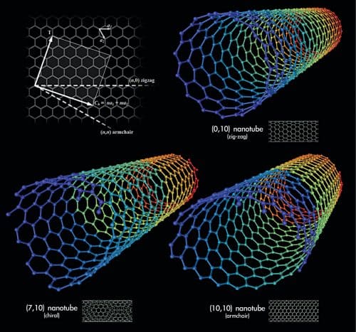
CNTs were introduced in 1991 by Japanese physicist S. lijima. CNT is a nanoscale tube that is made up of rolled sheets of graphene (see Fig. 1). It can be single-walled (SWCNT) or multi-walled (MWCNT). The SWCNT comprises a single nanotube, while MWCNT comprises numerous nanotubes with interlayer spacing of 0.34nm.
SWCNTs show properties such as semi-ballistic carrier transport and prevent short channel effects. These can be either semiconducting or metallic in nature. SWCNT is addressed by a whole number pair (n, m) called chirality vector. The nanotube is metallic if n=m, or n−m=3i, where ‘i’ is a number; in any case, the SWCNT is semiconducting.
Overview of 2 to 4 decoders
A decoder is a combinational circuit that converts or decodes the n inputs to 2n outputs. It is basically a multi-input, multi-output logic circuit that converts the input to output codes—keeping the input and output codes different. The input code mostly has lesser number of bits than the output. Decoder performs the function reverse to that of an encoder. There can be many types of decoders depending on the number of inputs available such as 2 to 4 decoder, or 3 to 8 decoder.
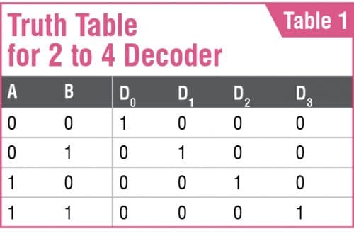
In 2:4 decoder there are 2 inputs and 4 outputs as can be seen in Table 1. In each of the cases any one of the outputs is set to 1 while others are set to 0. A transforming 2-4 decoder produces the reciprocal minters I0-I3, and accordingly the chosen yield is set to 0 and the rest are set to 1.
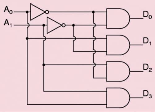
The 2 to 4 decoder (see Fig. 2) has two inputs A1 and A0 and four outputs D3, D2, D1, and D0. As a decoder, this circuit takes an n-bit parallel number and produces an output on one of the 2n output lines. The decoder comprises four AND gates and two inverters.
Using CMOS technology. While using CMOS technology, NAND and NOR gates are preferred rather than AND or OR gates as the latter require six transistors while the former require only four. This reduces the transistor count as well as overall efficiency. A 2 to 4 decoder can be implemented with four NOR gates and two inverters (see Fig. 3), that is, a total of twenty transistors.
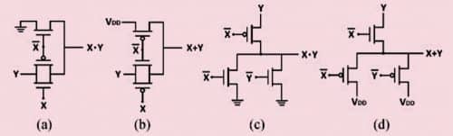
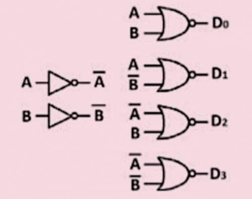
Using mixed logic. Transmission gates can be easily used to design the AND/OR gates as shown in Fig. 4, thus making the decoders efficiently. The mixed logic uses transmission gates and ‘pass’ transistors to implement a circuit. Pass transistor logic (PTL) was introduced in the 1990’s when many other designs were available in the market. It provides a suitable alternative to CMOS logic, keeping in mind the goals to improve factors such as speed, power, and area. The difference in such circuits is that the input is applied to both the gates as well as to the source/drain diffusion terminals of the transistors. The logic uses either individual nMOS/pMOS pass transistors or parallel pairs of nMOS and pMOS known as transmission gates.
The AND/OR gates implemented by the transmission gate logic are efficient and thus can be extended in the application of decoder. Fig. 4 shows 2-input AND/OR gates implemented using TGL logic. The figure shows that AND/OR gates implemented using DVL and TGL logic require only three transistors.
Proposed models for CNTFET based decoders
Fig. 5 shows the proposed 2:4 decoder using CNTEFT based technology. There are 20 transistors used in the circuit. The PMOS are changed to PCNTFET and NMOS to NCNTFET, respectively.
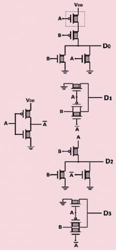
15T mixed logic decoder using CNTFET. The proposed circuit in Fig. 6 is for 2 to 4 decoder using the 32nm CNTFET technology. In this only one inverter is used, eliminating the use of Bbar as the input and thus only 15 transistors are used to implement the circuit. The D0 part in the circuit is basically in CMOS logic and the rest in DVL/TGL mixed valued logics.
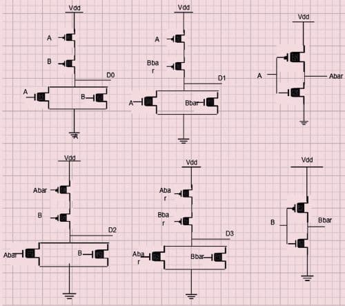
14T mixed logic decoder using CNTFET. Fig. 7 shows a two-input 2 to 4 decoder using CNTFET technology in 32nm. In this we mix TGL based AND/OR gates and DVL based AND/OR gates into one topology to form a 14T 2 to 4 decoder. The most important thing is that by combining we eliminate one inverter from the conventional 16T transistor topology, thereby reducing the total number of transistors as well as minimising the power dissipation.
We eliminated inverter B from the circuit and used DVL logic to implement D0 minterm in which A is used as a propagation signal and used TGL logic to implement D1 minterm in which logic B is used as a propagation signal. DVL logic is used for the minterm D2 in which A is the propagating signal and at last TGL is used to implement the midterm D3 where B is the propagation signal. As a result, the complementary B signal is completely removed from the logic circuit. Thus, transistors in the circuit can be reduced to 14 by removing the B inverter and so lowering the power consumption.
Results and simulations
All the circuits have been simulated in HSPICE with 1V supply voltage using a 32nm model for low-power applications. In each simulation average power, power dissipation, and transmission delay have been calculated. From these results the product delay has also been found out and compared.
Appropriate bit sequences are entered in the input to cover all possible transitions for the decoder. A 2-4 decoder has 2 inputs from which it can generate 22=4 different binary combinations. The 2 to 4 decoder is simulated for 500ms.
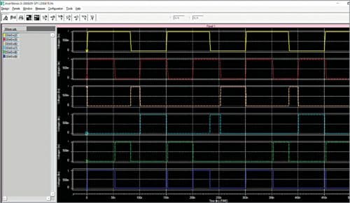
The waveforms in Fig. 8 show our proposed circuits using CNTFET working well and we compare their results in the following figures and tables.
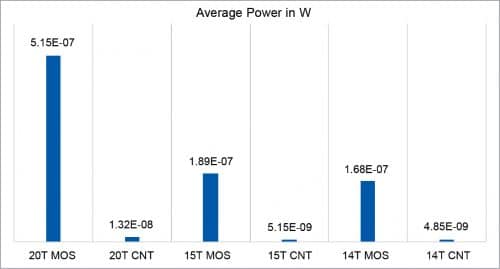
Fig. 9 shows comparison between the average power of MOSFET, CNTFET, and mixed logic decoder circuits. From the figure it can be seen that the average power consumption in CNT based decoders is very much less than in CMOS decoders, and the least consumption is in 14T CNTFET decoder.
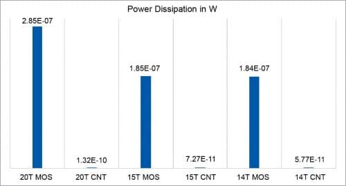
Fig. 10 compares power dissipation amongst MOS, CNTFET, and mixed logic decoders. It can be seen the power dissipation in CNTFET is very less as compared to MOS circuits and the 14T CNTFET (mixed logic design) decoder has the least power dissipation.
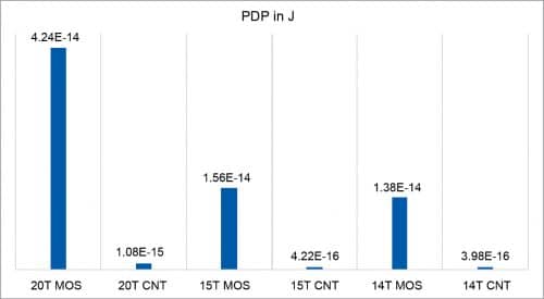
Fig. 11 shows PDP comparison between 20T CMOS decoders and mixed logic 15T and 14T MOSFET and CNTFET decoders. From the results we infer that the CNTFET based decoders are better than the MOSFET based decoders as all the CNTFETs yield better PDP than their respective MOSFET decoder. Moreover, the PDP is lowest for the 14T CNTFET decoder amongst all. Thus, it is the most efficient decoder as compared to the others.
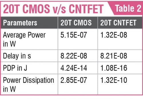
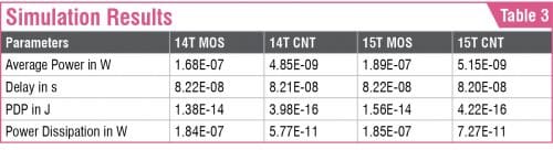
Simulation results for power dissipation, average power consumption, PDP, and delay are also shown in Tables 2 and 3 where CMOS based 2 to 4 decoder is compared with the CNTFET proposed 14T and 15T decoders.
In the 20-transistor model, according to the obtained results, CNTFET based 2 to 4 decoder presents less power dissipation, less delay, and a better PDP against the 20T CMOS based decoder. Thus, overall it outperforms the conventional CMOS based decoders in all respects.
Similar results are seen for the CNTFET based mixed logic designed decoders (14T and 15T) when compared with the CMOS based mixed design decoders. Although all CNTFET models have less power dissipation and PDP than the conventional CMOS, the CNTFET based 14T performs extremely well in comparison to all other models with least power dissipation, average power consumption, and PDP.
Conclusion
Carbon nanotube field effect transistor (CNTFET) is the best amongst upcoming technologies. However, as the quality of a CNTFET is not the same as of traditional mass-produced CMOS, there is need for new production techniques.
The proposed decoders were successfully simulated in HSPICE. The results obtained confirmed proper functioning of the decoder. It was found that the proposed CNTFET circuits consume much less power, reduce transistor count, and dissipate less power as compared to MOSFET based decoders.
Simulation results show that CNTFET 2 to 4 decoder in 20T, 14T, and 15T is better than MOSFET based decoders as average power requirement is reduced substantially. Also, there is significant improvement in the PDP and power dissipation voltage source when compared with an MOSFET decoder.
Therefore, we finally conclude that the mixed logic CNTFET decoder is very much effective for reducing the transistor count, average power, and power dissipation.
Jatin Gupta is PG Scholar, M.Tech VLSI, JC Bose YMCA University of Science and Technology. Prashant Kumar is Assistant Professor, Department of Electronics Engineering in that University at Faridabad


