
1. Complex double-patterning lithography
Complex double-patterning lithography in 20nm process requires rule-aware placement and routing in order to ensure the ability to colour mask correctly and efficiently.
Anil Kalra, senior group manager, Design Enablement & Services, STMicroelectronics, says, “With nanotechnology continuing to allow shrinking of semiconductor devices, VLSI design is becoming more and more exciting for designers. It is an amazing industry where people are continuing to bring innovative solutions for seemingly blocking challenges being faced along the way. Crossing the available litho limits with multi masks for a layer (dual and triple patterning) is becoming a reality—although at a price and increased complexity to be managed both by the designers and the manufacturers—possible only by close collaboration with EDA industry.”
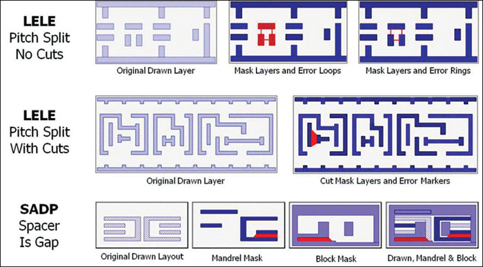
Jaswinder Ahuja, corporate VP and MD, Cadence Design Systems (I), president, VLSI Society of India, and former ISA chairman, adds: “One of the most difficult (and discussed) design challenges at 20 nm deals with the need for double patterning to overcome the limits of existing lithography equipment. It has such a pervasive impact on the silicon that every step in the design flow must anticipate and prevent potential problems. Standard cell development, placement, clocking, routing, extraction, timing and power analysis, and design-rule checking need to be ‘double-patterning aware.’ Therefore a unified, double-patterning-aware design flow across custom and digital domains becomes imperative at 20nm.”
The first thing affected by double patterning is cell and library generation. Designers need to make sure that the silicon IP is compliant with double-patterning layout rules. It is also critical to take double patterning into account during placement.

Cadence has developed a technology that automates colourised placement, resulting in a less congested design that helps meet timing and power requirements. However, the most important aspect is routing. Double patterning has to be integrated in the routing solution. It cannot be an afterthought where you complete routing and then run decomposition. It has to be done correct-by-construction and that is Cadence’s approach.
Cadence carries double-patterning intent forward from cell and IP generation to double-pattern-aware routing, and finally to signoff physical verification. This provides faster convergence because the intent is carried forward throughout the flow.
Andy Biddle, product marketing manager, Implementation Group, Synopsys, informs, “We have been working with the leading foundries and early adopter customers to develop an effective solution to this problem. We have made a number of enhancements to IC Compiler in order to ensure a fully decomposable design with minimal die overhead.”

To ensure minimal die area, there is much more than just making space between cells and tracks. Work starts with library preparation stage by analysing the library and identifying cells that are already DPT clean (cells that can be abutted to other cells). If the colour information is provided in the library, this will be used by the placer.
DPT clean means that the placer must ensure adjacent cells meet minimal space requirements if the boundaries are of the same colour or, if available, flip cells or select suitable alternatives, if available in the library. IC Compiler will use colour information available in the library to ensure compliance. IC Validator in Design, which has a foundry-certified colouring engine, is available within the IC Compiler environment to perform a fast check, if needed, during the implementation process.
The router needs to provide a two-colourable solution at the end of design while minimising the impact on area and runtime. The key to this is not just applying the DPT spacing rules blindly, which would ensure DPT correctness but also lead to area explosion. Zroute, the router within IC Compiler, utilises multiple techniques to ensure DPT readiness and applies them intelligently. One of the techniques utilised by the router is selective use of spacing rules and knowing when to apply which rules and when to apply other techniques. The second technique looks at routed patterns and ensures that there are no odd cycles or DPT violations created so that every route can go on an alternate mask.
The Synopsys Custom Designer tool for mixed-signal design provides a design-rule-driven layout capability that supports the new 20nm rules including spacing rules and new complex via requirements. This capability will significantly help designers of custom circuits comply.
2. In-design physical verification
20 nm involves in-design physical verification throughout the flow to reduce time-consuming, uncertain iterations. It is interesting to see what is being done in this area.
To provide designers with a complete end-to-end design and sign-off solution, Cadence integrates its physical verification system with industry-standard Cadence Virtuoso custom/mixed-signal and Encounter digital design flows, informs Ahuja.
