
When it comes to designing SMPS for electronic devices, big or small, wattages do affect as the components, layout, and topology change. As a result, the aspects to consider will also change. Paying attention to the upkeep of capacitors and related components along with resolving issues on electromagnetic interferences go a long way in tackling challenges filled with erroneous circuit challenges.
During SMPS designing, most engineers tend to overlook certain crucial aspects. After the process is complete, at first glance the design looks okay until an unstable power supply issue creates a problem in the entire product, leading to numerous complaints from the consumers. So let us take a look at these overlooked aspects and address them one by one.
The power supply is one of the most essential features of any electronic device, from lighting systems to consumer durables, or from industrial products to electric vehicles (EVs). The life of an efficient product stays in its switched mode power supply (SMPS). Designing an efficient supply not just guarantees stability in the complete circuit but also ensures the reliability of a product.
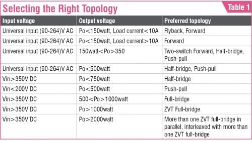
The wattage plays an important role in deciding the topology as per requirements. So, an isolated or non-isolated topology can be chosen as per the design specifications. Starting right from flyback at lower wattages to push-pull and full-bridge that are used widely in larger output requirements, many topologies exist in power electronics. But they all have the same factors for reliable output.

How to reduce capacitor failures
As per a study, about 17.1% of all failure is due to capacitor deterioration. The major culprits behind this are ambient temperature, capacitance, and voltage stress. Commonly observed capacitance failures include:
- Swelling
- Chemical leakage (which affects nearby components)
- Capacitor explosion
- Shortening
- Reduced capacitance (which affects the overall circuit performance)
- Increased in-circuit ESR
Certain preventive measures that can be taken are:
- Use high-quality capacitors
- Keep capacitors cool as much as possible
- Do not make ripple excessively stressed
- Keep in check the voltage stress factor (max. applied voltage divided by device nominal voltage)
A capacitor’s shelf life should also be considered, which is approximately two years.

Therefore, before using any capacitor, carefully check the capacitance value and its remaining life.
The reason why capacitors should be kept cool is that most SMPS inside cabinets are exposed to 45-50 degrees Celsius temperature. At that point, the failure rate of a capacitor increases drastically. By keeping the ambient temperature inside the cabinet/capacitor lower, the chances of failure decrease. Also, if you are using a capacitor at a higher temperature, then make sure that the capacitor is not very old.
When it comes to capacitor longevity, we generally go by whatever temperature is mentioned in the datasheet. However, we rarely check the reason behind its specification.
As per Arrhenius’ Law, the life of a capacitor becomes half with every 10°C increase in the ambient temperature. So, it should be a common practice to make the lifecycle calculation after the prototype by measuring the ambient temperature (and not just go by the specification mentioned in the datasheet). Only after that the SMPS lifecycle should be finalised.
Overlooked reasons for MOSFET failure
Some common reasons for MOSFET losses are:
- High drain current and voltage
- Incorrect heat-sink placement
- Shorting of legs
Problems can occur in MOSFETs due to a high rate of rise in drain-to-source voltage, causing a MOSFET to switch ON while it is switching OFF, which is dangerous. This happens because the gate threshold voltage typically reduces to less than 70% of its 25°C value at the maximum junction temperature. So, while designing, the important parameter to consider is temperature. The gate threshold voltage should be taken at the working temperature of the MOSFET and accordingly the ON-OFF switching process designed, so that no false triggering of the MOSFET occurs (while it is turning OFF). This will reduce the MOSFET failure to a great extent.
Other factors to keep in mind during placement of MOSFET in the design are:
- PCB creepage factor
- Correct placement of and height of legs near heatsink and in PCB
- Correct package
- Correct snubber design to avoid peak voltages
Lossless snubber design
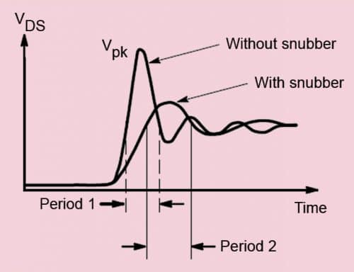
As seen from the graph in Fig. 1, without snubber the spike affects the circuit and damages the power switch. To mitigate this effect, a snubber circuit is used.
Snubbers are devices for suppressing voltage spikes and thus controlling the rate of voltage change. Clamps, on the other hand, are used only for voltage spikes and do not help in EMI. So, we choose them accordingly. They both have their uses, trade-offs. and circuit requirements.
You must have used snubbers several times. But I doubt you ever calculated the losses in them. Generally, we engineers tend to think that snubbers are here to help us. They are often thought to be more as saviours than culprits of power losses, but, in reality, the losses caused by them silently kill the circuit efficiency. So, if you have never calculated power losses that occur due to snubbers, don’t worry. Let’s check them here.
The formula for calculating power loss due to snubbers is:
Prs=0.5 . Vs2 . Cs . ƒsw
where Vs=Voltage across the snubber capacitor Cs
ƒsw=Switching frequency
There are two ways to achieve more efficiency in already-optimised circuits: either optimise the snubbers or use a lossless snubber.
A lossless snubber is a snubber whose energy is trapped and recovered by the power circuits. It is designed to absorb a fixed amount of energy and store that in a capacitor.
As seen in Fig. 2(a), the size of the capacitor decides how much energy the snubber can absorb and then give the same back to the circuit. The clamp circuit works by first absorbing the leakage energy in the clamp capacitor and then recycling it through an additional transformer winding, called the snubber winding. So, theoretically, no losses occur and whatever energy that has been captured is given back to the main circuit.
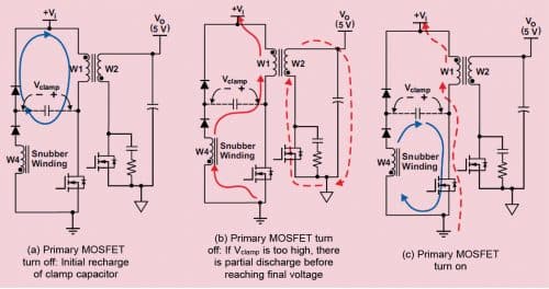
At the primary MOSFET turn OFF, the clamp capacitor is recharged until Vclamp reaches the secondary voltage reflected to the primary side.
In diagram (b), it can be seen that if Vclamp becomes too high, the excess energy is recycled to the output rail and the input bus (shown by the solid and dotted red-colour arrows).
In diagram (c), when the primary MOSFET is turned back ON, the clamp capacitor is discharged through forward coupling using snubber winding and primary winding. In short, the energy in the form of heat is trapped and recycled back to the circuit, making the complete circuit more efficient. That’s why it is known as a lossless snubber.
Optimise the magnetics
To ensure the efficient operation of SMPS, the magnetics have to be designed in a focused way. So, let us discuss it as winding placement can largely affect leakage.
We all know that the leakage inductance of primary winding should be low, but minimising the leakage inductance of low-current auxiliary winding to the primary is not a good strategy. The large leakage inductance of auxiliary winding to primary limits the energy delivered to these primary windings during commutation by increasing their CCM load range and improving their cross-regulation. The leakage should be less but for only primary winding, not for auxiliary winding. For this, we prefer to use sandwich windings.
As shown in the first block in Fig. 3, the W2 or the heavy loaded winding is sandwiched between the primary windings, which is a better alternative to the third option where the auxiliary winding is closely packed with the W3 winding.
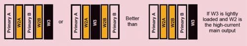
Another benefit of using the sandwich winding is that the auxiliary windings will be more coupled to the secondary windings, giving a tighter control for the system to optimise the output voltage sensing.
Various other factors that need to be taken care of during magnetics are:
- Try to keep your main winding fully loaded.
- The winding of the output with the widest load range (usually the regulated output) should have the best coupling to the primary, which means it should have the smallest leakage inductance to the primary. Primary should have the lowest leakage while auxiliary should not be considered to have low leakage.
- Use multifiller (side-by-side) or Litz wire for optimum efficiency.
- Operate the secondary auxiliary outputs close to the boundary between CCM and DCM.This ensures that enough energy but not too much is delivered to each. One way to accomplish this is by adding series impedance or by adding load current at minimum load.
- When secondary windings share the same ground and polarity, use an AC or DC stack. Either stack them just after the winding for AC stack or stack them after the diode to make DC stack. This would also improve cross-regulation.
- Spread the winding over the complete bobbin.
Solve EMI/EMC issues
As many electronics products work at proximity at different frequencies, a lot of interference occurs. It is to be ensured that none of these devices harm us or each other, for which the products should be EMI/EMC compliant.
Since the first thought for resolving EMI/EMC issues is magnetics, certain points need to be kept in mind:
- Always lay down the primary winding layer first, which starts at the MOSFET drain. The outer windings will act as a shield to the high switched noisy half of the primary winding connected to the MOSFET drain. Since the winding at the MOSFET has a very high noise while switching, because of which EMI/EMC issues occur, that’s why put the windings lower so that other windings cover it and shield the noisy winding.
- Always use a centre-gapped transformer. This is because there exists a fringing field, which causes magnetic flux leakage and leads to common-mode emission. For a centre-gapped core, the winding can act as a shield to the fringing field.
- Use shields in transformer windings. Adding a shield between the primary and secondary can reduce the parasitic capacitance. The shield can be added by winding an additional layer of wire covering the whole bobbin’s width. One end of this winding is left floating while the other end is connected to the primary ground.
- The use of the transformer flux band can further reduce the EMI generated by the transformer’s stray magnetic field. This flux band is grounded to the MOSFET ground through a small wire.
- Use snubbers on power switches for controlling both the spike’s transition rate and shape, and also the peak voltage. A high di/dt loop creates noise due to radiated magnetic fields. So, ensure that enough decoupling capacitance is present to filter away the high-frequency noise.
- Use high-frequency, low-impedance capacitors at both input and output of a transformer, combined with other types of filters and capacitors. Also, minimise the loop area of fast di/dt current paths, which can be done using toroidal-core inductor for output filters or by avoiding rod-shaped inductors that generate an H-field because of their open core shape.
- Pay attention to the reverse recovery catch diode characteristics, which can be a source of H-field emissions. Forward recovery, if too slow, will delay the transition time and increase the E-field emission. Although Schottky diodes do not have reverse-recovery issues, they have a parasitic capacitance that resonates with the parasitic inductance of the other components and PCB. If necessary, place an RC snubber across the catch diodes.
By following these steps, you will greatly reduce EMI/EMC in an SMPS.
Efficient PCB layout
If the base is not correct, then no circuit will work in the system. So, setting the base, that is, the correct PCB design, is highly important. A perfect SMPS cannot be made without a perfect PCB.
From Fig. 4(a) we can see that there are four main current loops. A and B are AC current loops with high di/dt. The other two are input and output current loops, which are at low frequency. Loops A and B should be laid first because they are high-frequency loops. Their tracks have to be wide and as small as possible, minimising the resistive and inductive effects on the components. The other two low-requency loops should be connected directly to their filter capacitor terminals; otherwise switching noise can bypass the filtering action and create conducting interference.
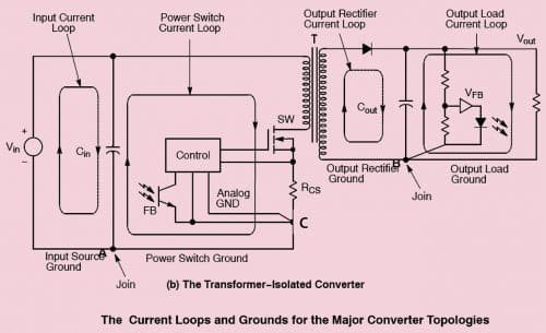
The word ‘Join’ mentioned at the bottom of the diagram refers to the points where ground tracks should meet both high and low-frequency sections (capacitor negative terminals), which is generally missed and leads to a lot of filtering and EMI issues. This can be implemented for both isolated and non-isolated circuits.
Another example is the transformer-isolated circuit to which the same rule applies here, that is, the same precautions need to be taken for isolated circuit components as discussed for non-isolated circuits.
Another important factor in PCB layout is ground. It is well known that ground is the main culprit behind every noise. However, it is also required as it forms the reference connection to the entire supply. Each ground has its own set of signals and can create a major problem if not connected properly.
In addition to the four ground loops that were previously discussed, there is a fifth ground loop, which is a low-level analogue control ground or controller ground, critical for proper operation of supply.
The word ‘Join’ (at the bottom-left in Fig. 4) indicates that the grounds, which form the major current loop, must be connected. Here, the connecting point between high-level AC ground, and input and output ground is the negative terminal of the filter capacitor to avoid EMI/EMC issues.
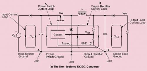
Next, the analogue control ground must be connected to the point where IC and its associated measuring circuit meet (indicated by C in Fig. 4(a) and 4(b)). If grounded above C, then any AC noise at large signals will sum up and can disturb the measuring of the control circuitry, which will impact the functioning of the overall system. Thus, the purpose of connecting the control ground at the lower side of the current sensing resistor or output voltage resistor divider is to form a Kelvin contact where any common-mode noise is not sensed by the control circuitry and does not impact the ‘brain’ of the SMPS. You need to sense properly for controlling the circuit.
So, these measurements need to be clear, and for that the grounding has to be very clean near the controller. PCB design is a critical factor in any design and should be done in a very focused manner to keep your designs running smoothly for many years.
Top mistakes, which designers make when designing SMPS:
- Not doing enough design simulations, which help a lot in designing circuits efficiently.
- Not doing proper calculations. (If you ignore them, you will face problems later in the production.)
- ‘Overdesigning’ SMPS for it to run longer. If you do correct calculations, you can derive the best value of each component.
- Improper testing.
The article is based on the talk ‘Designing Efficient SMPS: Core Of Everything Electronics’ by Nupur Jindal, a Power Electronics professional, which was presented at the March edition of Tech World Congress 2021. The article is compiled by Vinay Prabhakar Minj, a technology journalist at EFY.


