
 FM broadcasting is radio broadcasting using frequency modulation technology. In order to attain high-fidelity broadcast of music and speech, all audio frequencies up to 15kHz must be transmitted. The high fidelity FM transmitter presented here achieves that using simple and readily available components. Its output frequency is locked to 96MHz using the phase-locked loop (PLL) approach.
Circuit and working
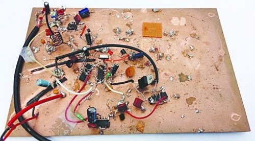
The author’s prototype of the high fidelity FM transmitter circuit wired on a copper clad sheet is shown in Fig. 1. Block diagram and circuit are shown in Figs 2 and 3, respectively. The circuit is built around dual D-type positive-edge-triggered flip-flop 74AC74 (IC1), ripple-carry binary counter CD4060 (IC3 and IC5), low-power audio amplifier LM386 (IC6), phase-locked loop CD4046 (IC4), 5V voltage regulator 7805 (IC2) and a few other components.
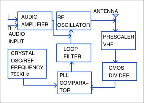
Transistor T1 along with resistors R1, R2 and R3, capacitors C2 and C5, coil L1, trimmer capacitor VC1, and varactor diode D1 forms a voltage-controlled oscillator (VCO) in Pierce configuration. IC1 acts as a VHF prescaler and divides the oscillator frequency by a factor of 4. Low-level RF output is taken via half-turn tap off L1 and fed to pin 3 of IC1 via C3 and to antenna via C4. The 24MHz (96MHz/4) output from the prescaler is further divided by 32 by binary counter IC3. This signal is available at its pin 5 (Q5).
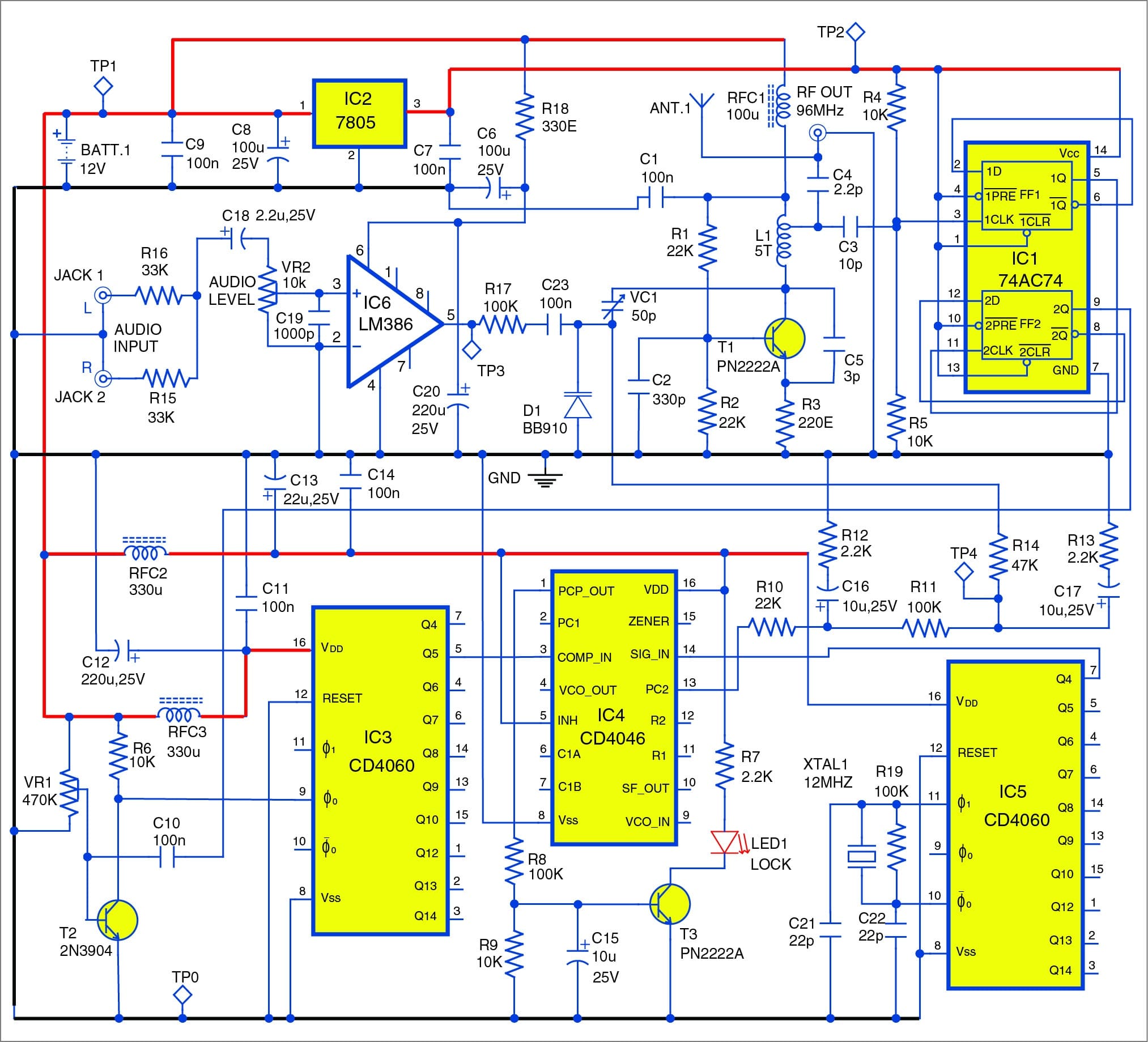
IC5 is used as a reference oscillator for the PLL, which generates a stable frequency of 750kHz at its pin 7. IC4 compares the two 750kHz signals presented to its pins 3 and 14, then decides the greatest frequency. The result is available at its pin 13, which switches between 12V and 0V.
Pin 13 of IC4 is coupled to a long time-constant filter formed by R10 and C16. C16 charges to the average DC voltage and so provides a control voltage to the transmitter’s oscillator frequency control circuit, and varactor diode via R11 and R14. R13 and C17 form another filter.

Both filters have damping resistors, R12 and R13, to reduce the control loop’s gain. Without these resistors the control circuit would over correct a frequency error, causing a larger and opposite frequency error.
The error signal from pin 13 of IC4 is filtered and coupled back to the varactor diode to correct the frequency. In effect, the oscillator is stabilised and referenced to a 12MHz crystal, giving the crystal stability. The oscillator, however, can still be modulated to ±75kHz (wide-band frequency modulation) with an audio signal. This would have been impossible if a crystal directly controlled the oscillator.

When the transmitter is initially switched on, allow a couple of seconds for the frequency to settle. This is a little annoying, but it allows the transmitter modulating frequency to be as low as 10Hz.
The stereo audio input is taken from audio jacks JACK1 and JACK2 and combined in R15 and R16. VR2 is audio-level control. The amplified audio frequency (AF) from IC6 is fed to the varactor diode via R17 and C23 for frequency modulation of the RF signal.
Connect a piece of wire (78cm long) to the RF output as an antenna. You may use an external RF amplifier at RF output to amplify the signal to 1W level.
Construction and testing
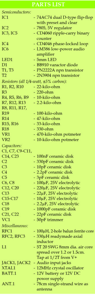
PCB layout of the high fidelity FM transmitter is shown in Fig. 4 and its components layout in Fig. 5. House the transmitter in a small plastic box. Keep all leads as short as possible. Use good-quality shielded cable for input audio connections. 12V DC regulated hum-free power supply is recommended.
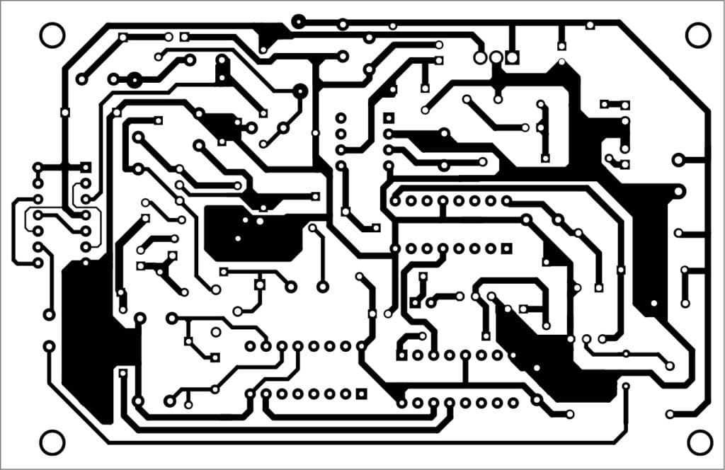
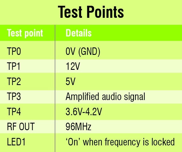
The operating frequency of the transmitter is 96MHz. Set VR2 to minimum and adjust VC1 for a reading of 3.6V to 4.2V at test point TP4. VR1 is biasing control for transistor T2 and should be set in the middle position. LED1 should light up to indicate a frequency lock at 96MHz. Feed audio signal at JACK1 or JACK2. This signal will be transmitted at 96MHz via antenna ANT.1. Tune the FM receiver to 96MHz. You should be able to hear the transmitted signal in your FM receiver. You can also use your mobile phone if it has inbuilt FM receiver.
Vary VR1, VR2 and VC1 for adjustment. For test points and troubleshooting, refer to test points table.
Download PCB and component layout PDFs: click here


will the circuit work?
Hi Deepak, the circuit is fully tested by our team and will work perfectly.
Yes it will work the first time. Author here. You can also substitute a ready made moulded choke for RFC1 (100 uH) or it can be replaced with a 22 ohm resistor. RFC2 & RFC3 can also be replaced with 22 ohm resistors. It helps keep unwanted RF out of the digital chips.
i have tried it in pcb but the TP1 is showing voltage in mV. RFC1 i have replaced it with 22 ohm will it work perfectly or their maybe any other issues with the circuit
Get in touch with me on email joy226010 at gmail dot com
Is it now working.
The circuit works perfectly. I have built many such units over the years for my friends. If TP1 is showing mV reading then there seems to be a short circuit somewhere. Check the 7805 voltage regulator. Touch all the ICs to check if any of them is hot to touch (indicating a faulty IC which has been short circuited). Also check the copper tracks of the pcb to make sure there are no wiring errors. Circuit will work. Also check your power supply. But a mV reading indicates a short. Also check all the transistors. You can use either RFCs or 22 ohms resistor, circuit will work either way. The RFC offers a large inductive reactance (resistance) to RF frequency of 96 MHz and very low resistance to normal DC voltage. Check all the components and wiring again. Make sure you check the power supply as well.
Can I buy this model or the prototype
Hi Sanju, You can avail a similar kit/ prototype at the link : https://grab.electronicsforu.com/products/quality-fm-transmitter
Hii, can you pls tell what will be it’s transmitting range in terms distance , I actually want it to be 200m.pls help
It will need an external amplifier for 200 m range. Email me at [email protected] and I’ll let u know how to achieve 200 m range.
Mail me
Hi
What is the power of this circuit?and
3 milliwatts
what is the kind of amper of antenna
what is the vc1=50pf trimmer?
what is the vr1=470kohm potmeter vr2=10kohm potmeter ? please explain its rolls?
I can see a problem in the circuit with VR1. When fully clockwise, it will pass full supply current through the B-E junction of T2 to ground. This will burn up the pot and likely the transistor too. A resistor in series with the base will fix this. Maybe 2K2, 4K7 etc.
Yes Dave you are right. Anothet flaw is that the CD4060 which is connected to 74AC74 prescaler isn’t dividing the 24MHz and the circuit failed to work when some college students made it in India. In the original prototype the CD4060 worked fine. I should have added another 74AC74 to bring the signal down to 6MHz and have it divided by 8 in a CD4040. What are your thoughts on this? I’ve used this new design in my 700mW FMTX and it’s working well. I’ve also used a 16V zener in place of varactor diode.
you mean this circuit doesnt work?
Maybe yes but the prototype worked fine
I tested that,CD4060 can divide 24MHz
but I have a problem
4046 doesnt work,I have two 750KHz in pin 3 and 14,but it doesnt locked and the voltage of test point 4 show me 11.6v
what should I have to do?
Hi Erfan, if cd4046 is getting the two 750KHz signal then it should be able to lock. Try changing the CD4046 and adjust the trimmer capacitor for PLL lock. The PLL led should glow constantly when CD4046 is locked.
Hi Joy,
Can you share 700mv FM transmitter circuit diagram?
Thanks
I tested that,CD4060 can divide 24MHz
but I have a problem
4046 doesnt work,I have two 750KHz in pin 3 and 14,but it doesnt locked and the voltage of test point 4 show me 11.6v
what should I have to do?
The cd4060 is not dividing 24mhz signal from the 7474 prescaler. The circuit will work if one more 7474 is added to bring the signal down to 6mhz then use a cd4040 for 750khz output to pll chip cd4046. In the original prototype cd4060 worked fine..
Hi Mr Mukherji. I havnt bb910 diode,I can replace a 16v zener diode?
Why I have in tp4 10.56 v?
I should be have 3 to 4v for lock frequence.
What’s problem?
Help me.
Hi every one.
I have a problem for locking frequence.
I see that the led for less than 1 second on. and quickly off at the same time in tp4 voltage increase to 10.56 volt.
I use svc202spa varactor diode instead of bb910.
Hi admin. I have a problem. I made this priject. When I want to test it, I have almoat 11.6v in TP4. However Ichanged the VC1,this voltage was fixed. What,s the problem. Pls help me as soon as possible!!!
Thanks alot.
Hi. Pls help me. Why the voltage of TP4 is fix in 11.6v and does,t change by adjust VC1?
Pls help?????
Hi Amir esmaeeli
Do you use varactor diode BB910?
I have your problem,11v in tp4.
I cant found a bb910 diode.
The LM386 isn’t capable of “high fidelity” – it’s noisy and distorted. You should use a good quality (and cheap) op-amp like the NE5532. You will have to develop a “midrail” to bias the op-amp, bt the results will be MUCH better!