
 Most of us leave our battery-operated devices like mobile phones, laptops, tablets, power banks and modems plugged into a charger overnight—even though these devices, especially smartphones with a quick-charge option, take about two hours or less to fully charge. After the device is fully charged, the charger remains idle for more than five hours (say, from 1 am to 6 am). Since we usually don’t access the Internet at night, modems too are just idling during this time, consuming some power.
Here we describe a power saver circuit for mobile chargers and modems. It is a simple op-amp-based multipurpose circuit that provides individual delays for your devices. After a specific amount of time, it automatically turns the devices off. This saves power wastage during idle time while increasing the operating lifetime of devices.
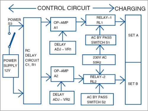
Block diagram of the switch box for mobile chargers and modems is shown in Fig. 1.
Circuit and working of Smart Switch Box
Fig. 2 shows the switch box circuit built around op-amp IC LM339 (IC1). IC LM339 consists of four independent precision voltage comparators. These comparators are designed specifically to operate off a single power supply. Two op-amps (A1 and A2) are used in IC1.
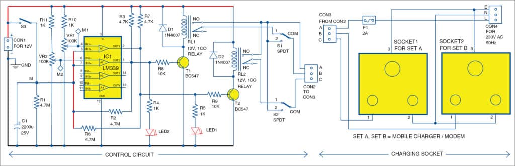
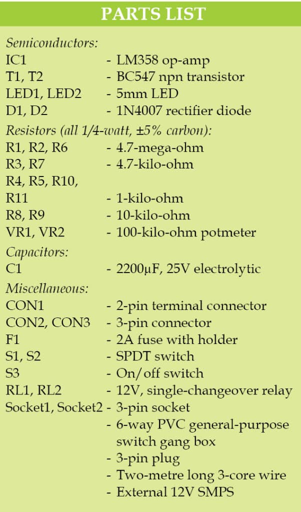
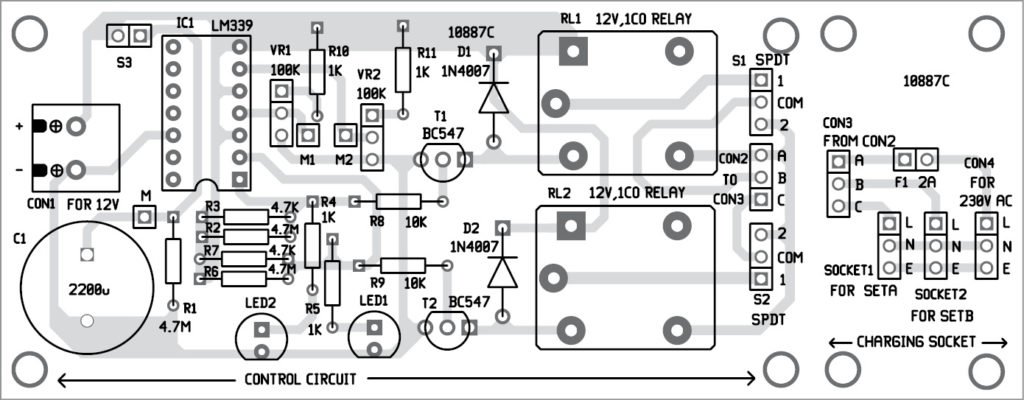
Here the switch box is divided into two different and independent sets (Set A and Set B) to control the charging. Each set consists of a 3-pin socket and is connected to a relay. Fuse F1 is used as a protection device.

The combination of resistor R1 and capacitor C1 in parallel forms the delay circuit. Here, a single R1-C1 circuit produces a common delay time for both the op-amps A1 and A2.
Switch S3 is used to charge capacitor C1 to 12V. When S3 is closed, the voltage at point M is around 12V. When S3 is open, 12V disconnects and capacitor C1 discharges through resistor R1. Point M is connected to pins 5 and 7 (non-inverting terminals of op-amps A1 and A2) of IC1. Potmeters VR1 and VR2 are connected to pins 4 and 6 (inverting terminals of op-amps A1 and A2) of IC1. Resistors R2 and R6 are used to provide feedback and stability. Resistors R3 and R7 are used as pull-up resistors. Pins 3 and 12 of IC1 are connected to 12V and ground, respectively.
LED1 and LED2 display the relay status. When S3 is open, the switch box operates normally and the delay circuit remains disabled. When S3 is closed and then opened, the capacitor discharges from 12V to 0V as the delay circuit is enabled.

The voltage at C1 (at point M) is given by the following relationship:
VC1= Vdc×e–t / R1C1
where Vdc is 12V.
When the voltage is set at M1 or M2 using the potmeter (VR1 or VR2), at the same time the capacitor also discharges slowly from 12V to 0V.
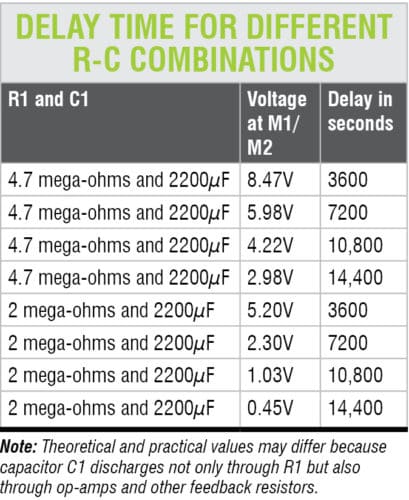
If the voltage at M>M1 or M2, op-amp outputs are high and relays energise, and vice versa. For example, if you want to de-energise relay RL1 after 3600 seconds (one hour), set the voltage at M1 to 8.47V. After 3600 seconds, the relay will de-energise, cutting off the voltage to Set A and Set B.
The table shows voltage values at point M1, M2 and delay time for different values of R1 and C1.
Switches S1 and S2 connect the line supply directly or through relays depending on their position. When switches S1 and S2 are in position 1, Set A and Set B get power supply through relays. When switch S1 and S2 are in position 2, Set A and Set B get power supply directly without relays.
During normal operation, switch S3 is open. Keep switches S1 and S2 in position 2 to provide line supply directly to Set A and Set B.
Construction and testing
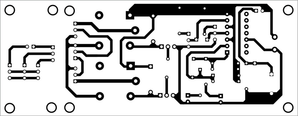
A combined PCB for the switch box circuit (including control and charging sections) is shown in Fig. 3 and its components layout in Fig. 4. You can easily separate the two PCBs. Enclose them in suitable boxes. Connect respective connectors between the control circuit and the charging socket.
Download PCB and component layout PDFs: click here
The circuit operates off 12V SMPS. A 3-pin plug with 2m long 3-core wire is used to connect the line supply (L, N and E) to the switch gang box.
Variable voltages obtained through the middle pin of potmeters provide different delays. Measure the voltage and calibrate the dials of VR1 and VR2 in terms of delay time. The accuracy of time depends on the tolerance of R1 and C1.
Connect CON2 and CON3 using male and female connectors, respectively. Connect 230V AC, 50Hz at CON4.
EFY notes
Since the assembled PCB is placed in the switch gang box, take care between AC and DC wiring. Use an appropriate fuse. Also, take care while connecting the relays. Use a 2-mega-ohm R1 in place of 4.7M if you want a different value as shown in the table.


in the description you are referring to on table but here its not there, Please share the table which is very important for us.
Thank you for the comment, we have updated the article with the table.