
 Here is a simple solid-state relay (SSR) driver circuit using a transistor. An SSR is similar in operation to a traditional electromagnetic relay with movable/physical contacts. It employs an optical semiconductor, called photocoupler, to isolate input and output signals; and switching elements such as thyristor, triac, diode and transistor. An important feature of this IoT project is that it does not use switching contacts, and so there are no physical wear and tear problems.
Circuit and working
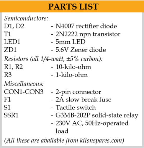
The circuit diagram of the SSR driver for the microcontroller (MCU) is shown in Fig. 1. It is built around two 1N4007 diodes (D1 and D2), 5.6V Zener diode, G3MB-202P SSR (SSR1), 2N2222 transistor (T1) and a few other components.
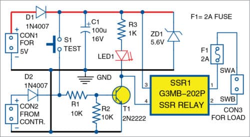
The circuit can be powered from a 5V DC supply. Transistor T1 and associated components, resistors R1 and R2, make it possible to accept DC control signal from other circuits like MCUs. Collector of T1 is connected to input of SSR1 to sink current from the positive rail, and its emitter is connected directly to ground rail.
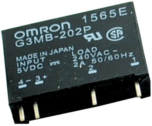
Resistor R3 is used to limit the operating current of LED1. Slow-blow (break slowly)—an essential component—2A fuse F1 is added for total safety. Similarly, diode D1 and Zener diode ZD1(optional) protect the remaining circuit. Image of G3MB-202P SSR used in this circuit is shown in Fig. 2.
Working of the circuit is simple. When MCU input is high, say, 5V, SSR1 gets activated and load connected across connector CON3 gets switched on. When MCU input is low, say, 0V, SSR1 gets de-activated and the load gets turned off.

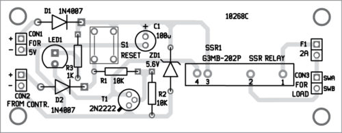
Construction and testing
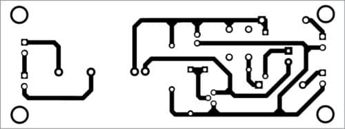
A PCB layout of the DC-to-AC SSR switch for MCU is shown in Fig. 3 and its components layout in Fig. 4. Assemble the circuit on the PCB. Connect 5V DC supply to connector CON1 to test the circuit and/or control signal from the MCU to CON2.
Download PCB and component layout PDF: click here
After successful construction, test the circuit by following the steps given below.
- Apply 5V DC supply to power input across CON1.
- Put digital multimeter into continuity or buzzer mode, and connect its test probes across switch-output CON3.
- Push test switch S1 to get sound on the multimeter. If sound is not heard, the circuit is most likely not working.
Otherwise, connect AC load to CON3. Load can be controlled by controlling signal input from the MCU at CON2.

T.K. Hareendran is founder and promoter of TechNode Protolabz


