

PHY is an abbreviation for physical layer of the conceptual open systems interconnection (OSI) model. With ever increasing demand for faster data transfers, over the recent times, the demand for hi-tech electronic products has considerably increased in India. Especially with introduction of the concept of the Internet of Things (IoT), where every device is connected to each other and to the Internet, there is growing need for enabling high-speed, high-throughput and high-performance systems.
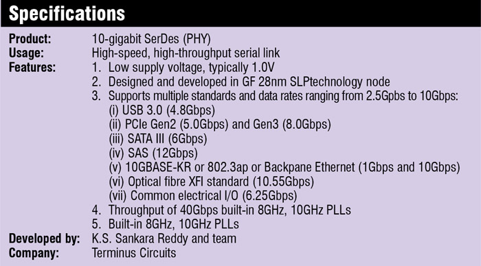
The multi-standard 10Gbps SerDes offered by Terminus Circuits is an off-the-shelf intellectual property (IP) offering that forms part of a main system-on-a-chip (SoC) or high-end equipment manufactured and sold by original equipment manufacturers (OEMs). It was designed and developed by K.S. Sankara Reddy, founder of Terminus Circuits, and his team in 65nm general-purpose (GP+) technology.
It is a PHY product that can support channels up to 32dB of attenuation, covering most of the cables supplied by the cable vendors. This multi-standard SerDes supports standards like serial ATA (SATA), serial attached SCSI (SAS), XFI, 10GBASE-KR, Peripheral Component Interconnect Express (PCIe) and universal serial bus (USB). This product forms the heart of high-speed and high-throughput servers.

The device is suitable for complex applications like weather forecast, brain simulations, high-performance computing (HPC), cloud computing and network operations centre (NOC). It can also act as enabler for SoCs targeting the latest standards like SuperSpeed and SuperSpeed+ USB (USB 3.1), PCIe 4 and applications like solid-state drives with native PCIE, terabytes routers, etc.
Design elements
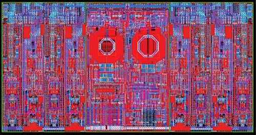
The analogue part of the transceiver is the physical medium attachment (PMA) that comprises custom-made transistors with a QUAD configuration for attaining high throughput (up to 40Gpbs). The clocking solution consists of three individual phase-locked loops (PLLs) that support data rates and standards ranging from 2.5Gbps to 10Gbps.
The digital side of the product, like Physical Coding Sublayer (PCS) and MAC (Media Access Controller) layer, consists of 500,000 standard cells connected for controlling and enabling the device connectivity between digital and analogue worlds, thus making the complete system that meets the standards mandated by various committees like USB.org, PCI-SIG, SATA, IEEE and SerDes.
The innovative design of this SerDes would help the OEMs in reducing the number additional off-the-chip components, such as high-precision resistors, clocking solutions and current-bias circuits. The complete solution is built on monolithic silicon as a single block. Thus the reduced number of external connectors and packaging complexities simplifies the test solution and reduces overall size, cost and power consumption of the system.


