

The primary motive of this article is to sensitise both hardware and software designers about the importance of designing testable products and how to enable low cost of testing.
In my more than three decades of experience, especially the last five years of working with startups and small and medium enterprises (SMEs), I have found that one of the important issues that most of them face is insufficient testing of embedded system products. They pay less attention to comprehensive testing of the products they develop, especially when the product has hardware in a fairly large amount.
An often-repeated statement is that it is impossible to test a product hundred percent. While this may be true to some extent for software in an embedded system, the hardware component has to be tested hundred percent to ensure the products are reliable and work as designed.

A second fallacy is to plan the testing of the systems after the design is complete; this never guarantees a fully tested product.
The third most common issue that I have noticed in my career is the complete ignorance of precision and accuracy of measuring circuitry. Almost all designers ignore that the system needs to be designed for precision and accuracy, and that the provision for calibration has to be in the design and not from provided components.
Many a time I have seen designers telling me that a certain issue be addressed by the manufacturing team. Manufacturing teams can only produce what you have given ‘as is’ and cannot improve the design.
This article highlights the need for understanding of testing of embedded systems at various stages. It covers the different types of tests that need to be done at various stages from development to manufacturing, and their importance. The idea is to help designers appreciate the value of the testing of embedded systems.
Anatomy of an embedded system
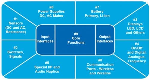
To understand the testing of embedded systems, we need to understand them at a high level. Refer Fig. 1 which shows the high-level functional blocks of a typical embedded system. Notice the testing of the system’s power supply and battery backup (#6 & #7)—most modern systems are battery backed-up systems and have become critical in the recent times. Remember that for a successful embedded system, every functional block has to be tested fully before it is shipped to the market. A typical embedded system has four major parts:
- Core of the embedded system is the electronics which can be a single printed circuit board assembly (PCBA) or multiple PCBAs.
- Mechatronics components like relays, motors, solenoids, etc.
- Displays and keyboards (typically mounted on the PCBAs, still tested separately due to their nature).
- Power supplies and battery systems used.
In addition to testing in the manufacturing line, designers have to test the product before the design is moved to the manufacturing line. These tests fall into two main categories:
- Design verification and validation tests.
- Compliance/certification tests which are typically one-time and done on a specific number of samples. Special code called field support firmware enables support engineers diagnose the system in the field to isolate the problem unit.
Types of embedded systems testing
When an embedded system is designed, designers need to understand the impact of testing on the product throughout its life. Embedded system testing is split into two major categories.
- Tests that are done once or twice during the design phase. These tests are controlled by the design team and are mainly firmware-focused. The design phase tests are non-recurring tests used by the designer to validate the system.
- Tests that are done in the manufacturing line. Every product is subjected to the tests and the number of tests depend on the product complexity and volume.
Non-recurring tests
Non-recurring tests are carried out on the prototypes and pre-release manufactured items to ensure the systems meet all the functionalities. There are two types of tests under this category.
- Firmware based solution which is typically developed by the designers to initially bring up the newly designed and assembled PCBAs. While this software typically helps to test all the CPU-accessible peripherals only, it is normally used to bring up the board and also validate the parameters of the PCBA.
- Tests that are conducted (non-recurring) to meet emission, safety, and environmental standards of different countries/zones where the products will be sold. This may involve developing a special firmware to maximise the emissions for compliance testing.
Recurring tests
Recurring tests are typically carried out in the manufacturing line and on every piece of embedded system that is assembled and shipped out. Fig. 3 shows the three different recurring tests at the manufacturing end—PCB assembly testing, sub-system testing, and whole product testing.
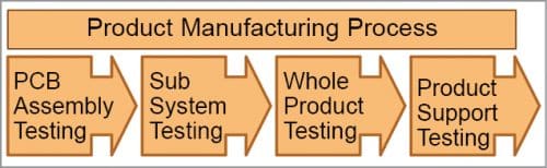
The fourth test, product support testing, is typically loaded into the system but will be used only by the field support team to diagnose the problems when the customer reports a malfunction. In the manufacturing line, this test is executed to ensure that the system is able to detect the components properly.
Now that we have seen the types of tests, let us see brief details of the tests.
Understanding the tests
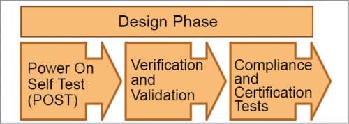
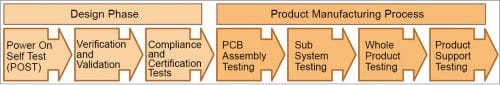
Fig. 4 depicts high-level development flow of embedded systems and the tests that need to be done in each of these phases. The key to understanding the tests depends on the design of the embedded system.
If an embedded system must be tested close to hundred percent, it is vital that testability be designed into the system right from the beginning. Planning to define testing after the design of the system is suicidal. Testability should be a must-have feature or requirement and not an optional one.
Designing a testable embedded system is essential for a successful product. Let us first see the different tests that have to be done before the embedded system is shipped out.
Fig. 4 shows that there are seven types of tests to be done in the entire product lifecycle. Each of them has a different purpose and has to be done differently.
A classic embedded system has seven tests in its full lifecycle in two phases. The first phase is the design phase where the embedded system takes the final shape from concept to final product. However, at the end of the phase, the product will be ready for transition to manufacturing after design verification and validation.
The tests carried out in the design phase are focused on validating the embedded system for its performance and functionality. The design phase tests are typically one-time.
However, the firmware developed for these tests will be used in the product subsequently for testing in manufacturing process and to detect any fault in its working during its life.
There are three types of tests that need to be done, but a well-designed code base can easily be customised to do the three tests that need to be done in the design phase. In the design phase, no special testers are developed, and only dedicated software/firmware are developed as design verification and validation needs sophisticated test equipment to validate the system to ensure the design parameters are validated.
Manufacturing tests address a different type of need. The manufacturing testers’ main function is to test every manufactured product completely, in a short time and at a low cost. In addition, the people who operate are technicians and not design engineers. Thus, the tests should be simple and deliver consistent results throughout the life of the product’s production.
Design phase tests
As we have seen in Fig. 4, there are three design phase tests that need to be done before the product can be moved to the manufacturing line for large-volume manufacturing. Design-phase tests are more programming intensive. The hardware has to be tested with calibrated test-and-measurement instruments for verifying the functionality and parameters.
The software/firmware that is developed has distinct uses. Let us see one by one. Since most current-day embedded systems are processor- or microcontroller (MCU) based, we can safely assume there is a need for design phase software/firmware development for testing the embedded system.
Board bring up code (BUC) and power-on self-test (POST)
These codes are dedicated software that will run in an MCU/processor-based board/system. A bring up code (BUC) is used to test a newly assembled board, section by section. BUC is typically interactive and user can feed parameters to vary the test data and exercise the newly developed board with various data.
Non-interactive version of the BUC is called POST or built-in self-test (BIST) and has a completely different use. POST/BIST is the first piece of software that will be executed in the manufactured product to diagnose the product every time the processor/controller boots up. It is shipped in every piece of product that is shipped out.
In the days of microprocessors (where all the memories and peripherals were separate devices), POST was critical as these components were external and many times from different vendors, increasing the need for critical testing. Best example of POST for microprocessors is the BIOS (basic input output system) in a PC.
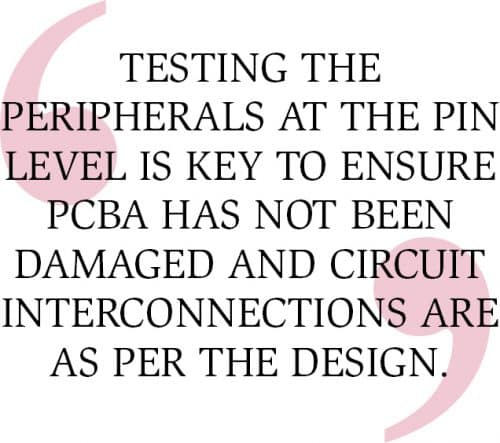
The biggest challenge in the case of a microprocessor with the peripherals being outside the chip is that the software developer has to develop the code that uses internal processor resources to first test the memories and then execute the full POST/BIOS from the memory. With the advent of microcontrollers, most of these memories and peripherals are integrated into the same device, making the POST development simpler. However, testing the peripherals at the pin level is key to ensure PCBA has not been damaged and circuit interconnections are as per the design.
One big challenge is the testing of analogue-to-digital converter (ADC) interfaces. ADC testing has two challenges—testing the basic functioning of the interface and the accuracy of the device. Most often, ADCs need a reference voltage and their functionality and accuracy is solely dependent on the reference voltage. Any change in the reference voltage can lead to system malfunction. Firmware developers who develop the BUC/POST code are required to have a complete understanding of the microprocessor/microcontroller and their peripherals, especially from the address map perspective, so that POST code is effective and compact.
As mentioned earlier, for bringing up a new PCBA, BUC is needed. Board BUC is basically the same POST code with interactive features. In fact, a smart firmware engineer can design a single firmware which can be either used as board BUC or POST, based on a dedicated signal from the board designer as an indication to the controller.
But we need to remember that a newly-assembled PCBA can have faulty interfaces, and this type of testing will be difficult if the device is defective or, in the case of microprocessor based systems, if there is a short in the PCBA forcing the POST code not to boot up. This situation calls for debugging with special tools, which is outside the scope of this article.
One of the common mistakes that hardware designers make is the lack of proper provisioning for programming the microcontrollers in the PCBA. There are no uniform programming techniques that device vendors follow. Most device vendors use serial interfaces like SPI and other similar interfaces, customised to their development tool. There are also third-party tool vendors who offer universal programming, but they are expensive.
However, the global standard seems to provide a JTAG port. JTAG port is a serial interface specifically designed for testing the ICs and PCBAs in the manufacturing line in a short time. Most IC vendors have used the same JTAG for programming the devices too.
One of the key facts that designers should consider is the programming, whether bulk programming is feasible and whether the product is expected to be made in large volumes. Ninety five percent of the designers or companies have never factored this into their design and end up spending a lot of time and money in programming alone.
Remember, if your software is frozen, your microcontroller vendor can offer a pre-programmed device for a small fee, saving you lot of effort and investment. But this is feasible only when your product is stable and no changes are envisaged.
The job of the POST code in an embedded system is to do minimum diagnostics in the version that has to be shipped. POST tests the memories and tests essential interfaces that are needed before the main software boots up and takes over. When the board is assembled and the hardware engineers are testing, board BUC is the key tool that helps in bringing up the board, and with a little tweak this BUC can be converted into POST.
Most companies never factor in that a PCBA bring-up is a joint effort between the hardware and software designers. The tool that connects them is the programmers interface document (PID).
PID is a simple document which lists the addresses and the corresponding device registers that will be accessed and also gives out the details of every bit in the register/memory and what action they will perform. This is a document which, if prepared during early design phase, can save plenty of time later.
Now a days, many microcontroller vendors do offer graphical utilities to configure a particular microcontroller and the tool produces the initialisation code either in C or in Assembly, which can be included in the main code base. If the designers use a single family of controllers, these BUC and POST can be re-used with little changes, and this mandates that the development of BUC/POST should be done with care.
Design verification and validation testing
The second test is for the purpose of design verification and validation (V&V). This V&V test normally is a customised version of the system software, while BUC/POST focus only on the correct functioning.
V&V test software will be a special customised version of system software. While system software is designed to maximise the performance meeting the design needs, V&V software ensures the system and hardware is fully tested for its functionality and weeds out the faults till all known faults are rectified.
V&V software is structured based on the product’s documented requirements. For domains like medical devices and avionics documenting, the test case against every known explicit and implicit requirement is a must.
This document is typically known as requirement trace matrix (RTM). Basically, this V&V software needs to test every requirement for its normal working and under fault condition.
Importance of testing during design phase
Testing during the design phase is important to ensure that the design is:
- Correct to the specifications and every specification is tested and proven
- Timing of the circuit is as per the design
- Components operate within the specified limits
- Validates the bill of material so that the costing is frozen
- PCBs and the systems can be moved to manufacturing after the clean-up of any corrections that need to be done.
We need to remember that BUC and POST alone will not test the system fully and we have to have the main software and simulated sources (for the sensors and input signals) to validate the whole system. While the design phase tests check the design, these cannot be used for manufacturing as it is, as the need for manufacturing tests are different. Some of the manufacturing test needs are:
- Every component needs to be tested individually before the assembled system is tested (this is not the case in the design phase test where the full product is tested).
- Test time has to be very short as with longer testing time product cost will go up due to increased manufacturing costs.
- Manpower available will not have any design knowledge and they are trained to use the tester and just log whether the system has passed the test or not. This means the tests have to be simple with a Go-No Go type of interface.
- Manufacturing tests have to log the test status data automatically without manual intervention so that the tests are efficient and the data is used to control the process.
Before delving into the details of manufacturing tests, let us understand the primary difference between the design phase tests and manufacturing tests.
Design phases are:
• Detailed and exhaustive to ensure the product in its design phase is tested fully for its functionality, performance, and reliability.
• How long the testing takes is not an issue, but the key is that the coverage of the tests should be hundred percent.
• As long as product designers retain the processor/controller from the same family, the POST/BUC tests once developed need only minor changes for the new design. However, the needs for the manufacturing tests are completely different and call for new test jigs.
Manufacturing tests
The primary requirement for testing of products in the manufacturing phase is to ensure the following:
- Every product is tested so that any failure due to component failure and process defects during assembly are detected and weeded out.
- Test the product in the shortest time to improve the manufacturing productivity.
- Ensure every product tested performs consistently and repeatedly without degradation in performance.
- Ensure every product is calibrated so that it meets the accuracy needed.
- Finally, ensure the cost of testing is kept low to keep the product cost low. Typically, the contribution of testing in product manufacturing is roughly 12-15 percent. Every percentage saved will be a big saving.
Remember that unlike the design phase testing, which is executed one or two times, every product that is produced in the manufacturing line is tested. This means the testing cost in the manufacturing line is a recurring expense and has to be kept minimal. This also means that testability has to be built into the design so that product can be tested fully in the quickest possible time.
Above all, note that in the manufacturing tests the testers may need changes every time the product design is changed. It is even more important that the design has to be stable so that cost incurred due to tester changes are minimised.
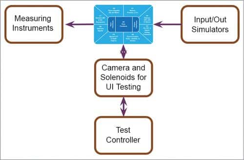
A typical embedded system test philosophy is based on four critical blocks as shown in Fig. 5. A typical manufacturing tester has:
- Test controller which could be a custom-made processor board or a platform like LabView from National Instruments (NI). NI offers a complete package with both hardware and software to create a tester in a modular fashion.
- Set of voltage, current, and signal sources which generate the signals needed to feed the embedded systems and can be controlled by the test controller.
- Set of measurement units which are controlled by the test controller and reads output from the embedded system under test.
- While generation of signals addresses the input and output of products, user interfaces like keyboards, knobs, levers, and displays such as LCD and LED need special visual equipment like camera with image processing capability, solenoid, and robotic units for operating the switches, knobs, etc.
While these four modules are pretty much common to any embedded system testing, how the testers are built, configured, and used depends on the manufacturing phase of the embedded system. Let us briefly see the different testers that are used in different phases of the manufacturing process.
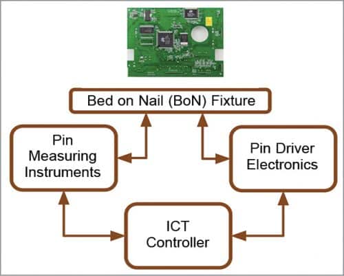
Electronics PCBA testing: in-circuit testing
Referring to Fig. 3, we can see that there are four stages of testing needed before the product is shipped out. In the first stage, the PCBA (raw PCB loaded with the components and soldered) is tested independently. This test is done when the board comes out of the soldering stage in the manufacturing line (after the inspection for any visible defects).
However, just PCBAs alone do not make the full embedded system as there are many more components needed. This essentially means that there are further processes after the PCBAs are tested.
The PCBAs have to be tested individually before these are assembled into the full system. Due to this, PCBAs are tested using in-circuit tester (ICT).
In PCBA stage, only limited functionalities of the overall system can be tested. Additionally, PCBAs may have connectivity issues due to imperfections in the soldering process.
In-circuit testers focus on testing the components and interconnects in the PCBAs. This ensures all the components soldered in the board are working and also that the traces between the components are soldered well and working before it is integrated into the system.
We need to remember that ICT-tested PCBA does not guarantee that the final product will work when assembled fully as there are other components like cables, displays, keys, and power supplies which also need to be tested and faultless. ICT testing ensures that the PCBAs are tested to be free of defects before these are assembled into the system.
In-circuit testers operate on the principle of back-driving (apply stimulus) and measure the response from the node that is tested. Fig. 6 shows a simplified view of the in-circuit tester. These are similar to generic tester in architecture. They have a set of pins to drive the signals and a measuring circuit connected to the same pins to read the response.
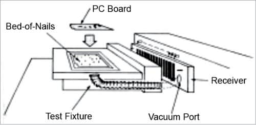
A unique feature of the ICT is that the PCBAs are tested using pins in the test fixture, which directly probe the test pads provided in the PCB for testing. For every unique PCBA, a fixture has to be developed to access the test pads provided through spring-loaded pins called pogo pins (named after the pogo sticks that children use for jumping and playing).
Fig. 7 shows a typical pogo pin cross-section and the cross-section of how the bed-of-nail jig is implemented for better understanding. Structure of the test jig has three components—a base plate in which the pogo pins are located at the locations where the PCBAs under test have test pads, a connection termination board where the pins are connected to the ICT drive and measurement electronics, and a vacuum cover which presses the PCBAs down on to the pogo pins during the test process. Fig. 8 shows the concept of ICT test fixture and a typical ICT tester for better understanding.
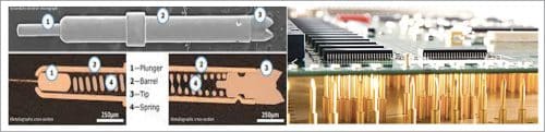
Since the ICTs use a plate with pogo pins for testing, they are also called bed-of-nail (BoN) testers. These pins are colloquially called nails!
Tester vendors provide test libraries and ICT test program developers use these to write the test program to test the PCBAs. The biggest advantage of ICTs is that they eliminate nearly hundred percent of the faulty PCBAs before they go to the next stage in the manufacturing line.
ICTs operate on the principle of comparing the signatures captured from a set of good tested boards called gold boards and compare the results with the boards under test.
These ICT testers are expensive. A new BoN jig has to be developed with corresponding test program for testing every new version of the PCBA, which increases the manufacturing cost.
One strategy is that for low-volume products, the ICT phase is skipped and designers use functional testers to test the product post assembly. While the risk of a faulty PCB leading to test-failure is high, the costs can thus be kept down due to low volume.
Sub-system and assembled product testing – ATE
The second and third tests cover the sub-systems and systems. These tests are executed by specially built custom testers that are specifically designed for the sub-systems/systems. Typically, a fully-assembled product testing involves creating the exact use-case situation with the tester and tests the product for its functionality, performance, and its fault-handling capability. Most of the ATEs (automatic test equipment) designed for this testing are hundred percent custom designed. The only common thing is that they may be built using platforms like LabView software along with compatible hardware modules.
With the emergence of scripting languages like Python, developers use open source software and custom hardware to build testers to keep the costs down. One lacuna seen with startups and SMEs is not adding a few hooks in their design, which leads to an expensive tester. A good example of test hook is the calibration signal output connector provided in most of the oscilloscopes, which enables the user to check by just connecting the probe to the signal generator (square wave of 1kHz @ 1V or 5V) pin provided for self-checking.
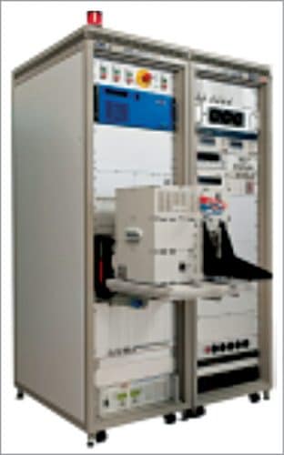
Except for software platforms like LabView or HP Vee, ATEs will be fully customised to suit the product that is under test. In the case of ICT, the tester and the fixture base remain the same except the BoN fixture and the ICT software which changes depending on the PCBA tested. Fig. 9 shows a typical view of an ATE.
ATEs are used for both sub-systems as well as finished systems. One of the key aspects most designers miss is that with a little design effort, the testing of the PCBs or systems can be easily implemented in a simple way at a lower cost.
Standard compliance testing
With increased globalisation, embedded systems are finding markets globally. However, each country or continent tends to have specific standards for electrical safety and electrical emissions and susceptibility. Products have to be designed to meet these standards before they can be commercially sold in the respective regions.
These tests are typically done by specific certified test labs. However, the onus of the product meeting the requirement is on the designers as well as the manufacturing partner.
While these tests are typically carried out one-time with the products, regulatory agencies like FCC, CE and VCCI periodically get sample products from the market and test them for compliance to the standards. Any failure to meet these tests will result in these agencies suspending the product sale till the problems are rectified. This forces the designer to design the product with sufficient margins to address the process variations in the manufacturing line.
How testing impacts products
The quality of testing impacts embedded systems in multiple ways. The ‘rule of ten’ explains this impact graphically. This rule is derived based on historical data and is shown in Fig. 10.
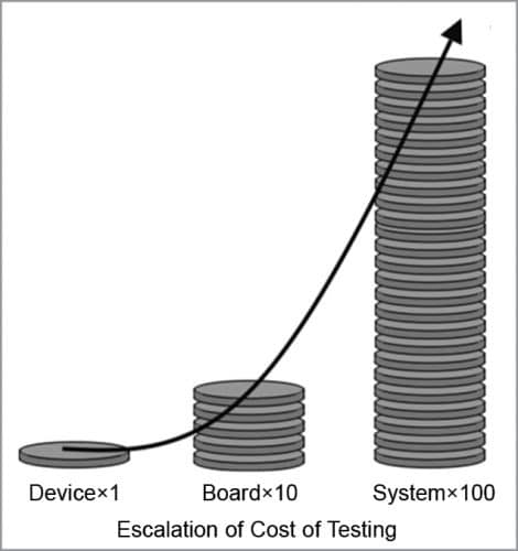
We can see that if a component failure is detected early on, the cost is just the failed component and test charges related to the test. When the same component failure is detected in assembled board, the cost of testing goes up ten times (component cost + assembly cost+ ICT test cost). And if the same problem is detected in the system, either in the manufacturing line or in the field, the cost is one hundred times.
This shows the importance of testing and complete testing of a product helps the product maintain quality at a low price. An insufficiently tested product results in:
- Product’s failure in the customer’s place, leading to customer dissatisfaction.
- Increased product support costs and repair costs.
- Company’s brand gets damaged due to failures.
- This issue gets aggravated when the product is from a startup or SME who is in the initial phases and may not have a big support network. Any field failure can result in customer dissatisfaction. As a result, most pilots do not go to the next stage and the product is deemed as a failure.
- Insufficiently tested product results in reduced sales and damaged reputation, something small companies and start-ups cannot afford. They should not rush to market with a poorly-tested product due to pressure. The key here is that designers plan and implement test hooks which increase the testability of the product and reduce failure with simpler testers.
Conclusion
Here, we have seen the different tests that an embedded system has to undergo and the different types of tests that are needed for the same. We also saw how the testing of embedded systems impacts product quality and functioning.
The primary motive of this article is to sensitise both hardware and software designers about the importance of designing testable products and how to enable low cost of testing. Unfortunately, academic courses do not teach these as the courses are focused on learning the fundamentals. Further, academic courses cover processors and controllers that are no longer in production, leading to a gap.
In my next article, we shall discuss how to implement testability in the design of embedded systems.
S.A. Srinivasa Moorthy is director at D4X Technologies Private Limited


