

In PCB layout designing, especially for BGA (ball grid array), the PCB fanout, land, and via are particularly important. Fanouts are traces from the device lands to adjacent via, as shown in Fig. 1. A via is an electrical connection between layers in PCB to connect the input and output, power, and ground tracks.
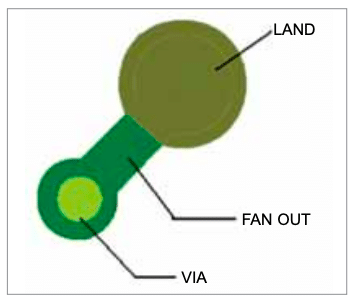
Typically, there is one via per land. PCB lands are where device balls sit and get soldered to. One of the important and difficult aspects of PCB design using fine pitch BGAs is the layout of their lands and fanouts.

Can we place a via under the BGA pad without fanout?
You can place a via under the BGA pad without fanout, but it comes with advantages and disadvantages. Having vias placed on a pad is a common practice. Some designers place vias next to a pad, in some cases even by removing some pads from the BGA footprint. Here fanouts are not involved.
If there is a via in pad (Fig. 2), it needs to be filled either with copper or non-conductive material. Because an open hole would cause the solder to flow away from the pad, which is not desirable. This via creates an extra step in PCB manufacturing and involves additional costs. That is why many designers don’t use this option.
The second problem is the required drill-hole diameter. For example, it is difficult to place a 0.2mm hole in a pad of a 0.4mm spaced BGA. Using a smaller drill size would result higher costs. One of the solutions is to use normal fanout routing with few vias. This option would give you a much cheaper solution.


