

Why do we need another form of electronics? Standard silicon-chip-based electronics is making great strides in miniaturisation, cramming more functionality into smaller chips. Couldn’t we just embed these chips into flexible materials to create flexible applications?
Answer is No. New applications like organic light-emitting diodes (OLEDs) and organic photovoltaics (OPVs) need big areas. “With silicon-based circuits, you would need huge numbers of embedded chips to get the necessary intensity and uniformity. That would be prohibitively expensive and would generate so much heat locally, you would melt the substrate!”
Flexible electronics could transform the way we make and use electronic devices. Flexible electronics opens the door to foldaway smartphone displays, solar cells on a roll of plastic and advanced medical devices—if we can figure out how to make them. Nearly everyone knows what the inside of a computer or a mobile phone looks like: A stiff circuit board, usually green, crammed with chips, resistors, capacitors and sockets, interconnected by a suburban sprawl of printed wiring. What if our printed circuit board was not stiff and was flexible enough to bend or even fold?

Why flexible electronics
Flexible electronics is in vogue for two reasons. First, it promises an entirely new design tool. Imagine, for example, tiny smartphones that wrap around our wrists, and flexible displays that fold out as large as a television. Or photovoltaic cells and reconfigurable antennae that conform to the roofs and trunks of our cars. Or flexible implants that can monitor and treat cancer or help paraplegics walk again.
Second, flexible electronics might cost less to make. Conventional semiconductors require complex processes and multi-billion dollar foundries. Researchers hope to print flexible electronics on plastic film the same way we print ink on newspapers. “If we could make flexible electronics cheap enough, you could have throwaway electronics. You could wear your phone on your clothing, or run a bioassay to assess your health simply by wiping your nose with a tissue,” Gomez says.
Before any of this happens, though, researchers have to rethink what they know about electronics. None of the flexible electronic devices under development would match the billions of transistors that now fit on silicon chips, or their billions of on-off cycles per second. They would not have to. Despite the challenge, flexible electronics promises changes that go beyond folding displays, inexpensive solar cells, antennae and sensors. It could veer off in some unexpected directions, such as helping paraplegics walk again.
Applications in health care
optical micrograhy of a flexible battery
during flexing
Flexible electronics has attracted a lot of attention for its enormous potential in many important applications, such as wearable health monitoring devices and medical implants. While a number of approaches to making flexible sensors or electronics have been developed over the last two decades, flexibility in electronic materials is very attractive for medical and bioengineering. Living organisms are intrinsically flexible and malleable. Thus, flexibility is a necessity for successful integration of electronics in biological systems. Furthermore, in order to carry out daily tasks, flexibility is less likely to hinder over stiffness.
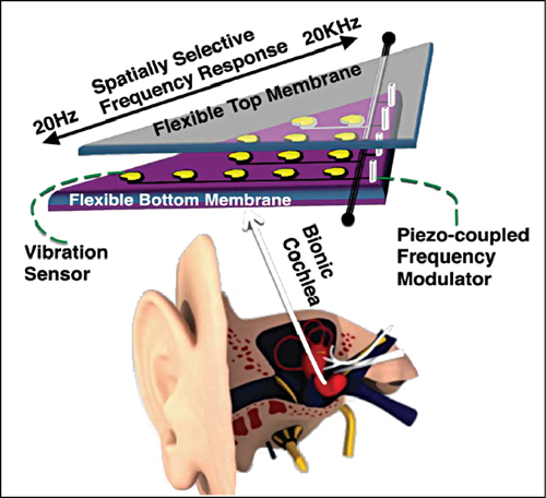
Recently, some electronic devices have been integrated into human bodies. One example is the bionic eye. Here a vision-compromised patient requires an electrically-active addressable matrix array, with each unit or pixel recording an image and transmitting this to the patient via the optic nerve. Such technology is not restricted to vision and is applicable to many other types of sensation.
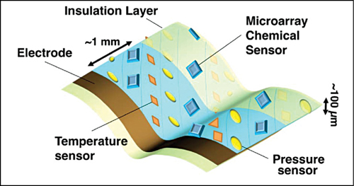
A microarray thin film can also be integrated into bed linen and patient dormitories, and can operate in similar ways to monitor and identify abnormalities in body temperature, as well as sweat-elemental analysis. As with the lab-on-a-chip (LOC) applications, these thin films will become a key component of our approach to next-generation healthcare. Heat distribution in the body, sweat content and frequency or postural pressure on part of the body can all reveal vital information on pathological symptoms or recovering stages.
Further applications of microarray systems based on such flexible thin-film technology are a facilitator for artificial noses and tongues, as shown in Fig. 11. Sensory receptors in olfactory (nose) and gustatory (taste) systems have a range of chemical receptors. Many of these receptors sense particular chemical properties, including acidity, salt concentration and enzyme affinity.
It can also be used to monitor the pulses from brain and analyse the changes and design the treatment based on the present situtation of the patient.
In automotive industry
The combustion reaction has fueled the development of humanity since the discovery of fire. The main reasons for the ubiquity of combustion are twofold. The first relates to its intrinsic mass and volume energy densities. For example, one kg of crude oil contains nearly 50MJ of chemical potential energy. The second relates to storage and portability. Crude oil happens to be liquid at surface conditions, making it easy to store, transport and convert, which is fundamental for applications such as transportation.
Although electric vehicles trace their invention to the mid-1800s, their widespread adoption has not yet materialised. This is partly due to the high energy density (J/kg) of fossil fuel compared to the batteries, with the implication that electric vehicles require unfeasibly heavy and large batteries to store equivalent energy as a tank of fuel. Besides low energy density, batteries suffer from low power density (W/kg), leading to electric vehicles with comparatively low performance when compared to equivalent fuel-powered vehicles. Despite these issues, increasingly scarce fossil fuel resources, as well as environmental incentives, have increased the adoption of electric vehicles, fueling research and development in this field.
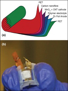
Advances in thin-film battery technology through the use of nanostructures for enhanced energy density and hybrid supercapacitor allowed increased energy and power densities. Lightweight substrates, such as polyethylene terephthalate (PET) and paper, have led to a reduction in battery weight. Flexible, thin-film technology is especially beneficial in this instance, as it allows batteries to be moulded into suitable shapes at relatively low costs.
Flexible thin-film technology may also find applications in road signs and markings. Intelligent roads will be engineered with the aim of improving road safety, lowering road congestion and energy consumption. The road and vehicle will be able to interact to dynamically adjust either party to energetically optimise their systems. The advantage of flexible thin-film technology is its mechanical durability and ease of inexpensive integration within the existing road networks.
In energy management and mobile devices
The innovative gadgets that we are presently experiencing are made possible by flex circuits in the industry. Today, mobile and other electronic gadgets manufacturers are designing the products keeping in view the future scope of the product and its use in more than one way. The ease of handling the device is also an important factor that needs to be noted while manufacturing. Now-a-days the devices are manufactured in such a way that these are embedded in our daily life beyond the limit of separation.
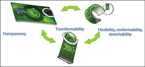
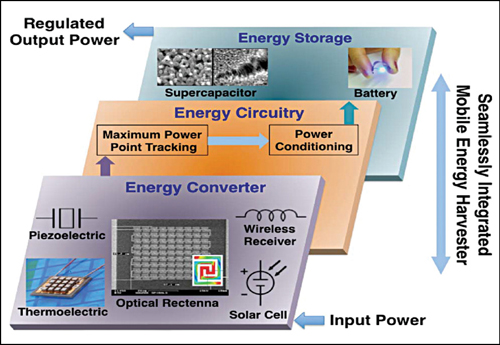
Nano-optoelectromechanical systems (NOEMS) could access energy sources arising at the nanoscale, converting energy from environmental sources, such as ambient noise or electromagnetic radiation, to mechanical vibrations. This route opens up many possibilities where device deformation allows for transformability and new paradigms of user interaction, such as in the Nokia Morph Concept.
There are different ways to harvest or scavenge energy from the surrounding or ambient environment, such as the collection of low-frequency vibrations, heat (via temperature gradients), biomechanical motion and solar energy. Among these, solar energy is perhaps the most promising.
Silicon is by far the most widely used photon absorber and currently dominates the market of PV devices, with an energy conversion efficiency (η) of up to 25%. Despite significant development over the past decades, the high cost of Si-based solar cells is still a bottleneck for the implementation of solar electricity on a large scale (in the absence of government subsidies). The development of new materials and concepts for PV could be a way to reduce the overall production costs, as well as increase efficiency. The latter is crucial in view of applications in mobile devices that have a limited surface area.
Thin-film solar cells, such as silicon, cadmium telluride (CdTe), copper indium gallium diselenide (CIGS) and thin-film crystalline silicon are termed ‘second-generation PVs.’ The development of thin-film solar cells has been driven by the potential of cost reduction in manufacturing. An even cheaper and versatile approach lies in the exploitation of organic photovoltaic (OPV) cells and dye-sensitised solar cells (DSSCs). These can be manufactured economically compared with silicon cells, for example, by roll-to-roll processing, even though they have low η.
In displays and human-machine interactivity
One of the most demanding applications of flexible electronics is in OLED displays. An OLED is a light-emitting diode (LED) in which the emissive electroluminescent layer is a film of organic compound that emits light in response to an electric current. This layer of organic semiconductor is situated between two electrodes. Generally, at least one of these electrodes is transparent. OLEDs are used to create digital displays in such devices as television screens, computer monitors and portable devices like mobile phones and PDAs. A major area of research is the development of white OLED devices for use in solid-state lighting applications.
There are two main families of OLEDs. Those based on small molecules and those employing polymers. Adding mobile ions to an OLED creates a light-emitting electrochemical cell or LEC, which has a slightly different mode of operation. OLED displays can use either passive-matrix (PMOLED) or active-matrix addressing schemes. Active-matrix OLEDs (AMOLEDs) require a thin-film transistor backplane to switch each individual pixel on or off, but allow for higher resolution and larger display sizes.
An OLED display works without a backlight. Thus, it can display deep black levels and can be thinner and lighter than a liquid crystal display (LCD). In low ambient light conditions, such as a dark room, an OLED screen can achieve a higher contrast ratio than an LCD, whether the LCD uses cold-cathode fluorescent lamps or LED backlight.
e-skin for human-machine integration
You might think that temporary tattoos look cool, but what if they could also collect and transmit information about your heart rate, temperature, muscle contractions or brain waves?
A new flexible electronic circuit promises to do just that, by moving with the skin and staying in place without any adhesive. The research used existing semiconductor technology to imprint integrated circuits onto a thin, flexible silicon film that can be applied directly on the skin. With the interactive e-skin, we could form an elegant system on plastic that can be wrapped around different objects to enable a new form of human-machine interface.
In addition to giving robots a finer sense of touch, the engineers believe that the new e-skin technology could also be used to create things like wallpapers, which double as touchscreen displays and dashboard laminates that allow drivers to adjust electronic controls with the wave of a hand.
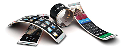
The mobile revolution has been won, but the smartphones and tablets that launched it have remained pretty much the same throughout. In 2013, we saw the emergence of flexible display screens as a viable option for personal electronics. And once the technology is perfected, the range of possibilities gets a whole lot broader. How about a T-shirt that plays YouTube videos? Or a 229cm (90-inch) high-definition TV which you can fold and bring to a friend’s house for the big game? All are starting to seem like real possibilities.
The breakthrough came as researchers like those at Colaneri’s lab figured out how to build display panels onto paper-thin plastic substrates—thin slices of material that act as semiconductors—instead of glass. “We’ve always said that flexible displays are sort of the beginning toward truly flexible electronics,” he said. “The display in a conventional phone or laptop or tablet is the least flexible thing in there, since it’s made out of a piece of rigid glass.”
The first wave of consumer gadgets using that and similar technologies is under way, with more promised in the near future.
Korean gadget giants Samsung and LG have already rolled out TVs and phones with curved display screens. Apple has filed for a patent for an ‘electronic device with a wraparound display.’ At Google, one of CNN’s Thinkers, Mary Lou Jepsen, is a pioneer in the field of display screens. She’s in the super-secret Google X lab, so there’s no telling what she and others are actually up to. But it’s hard to imagine new displays aren’t somewhere on the agenda.
“All of the names that you mentioned are certainly sniffing around (the idea),” Colaneri said. “I think all of the names that you’ve dropped are also among the top-ten list of most paranoid, secretive organisations known to man. They’re certainly thinking about it.”
Conclusion
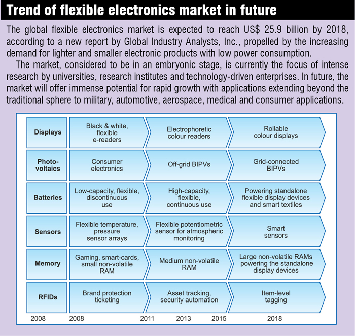
Flexible electronics is an emerging field of science and manufacturing technology, which enables planting of electronic devices onto conformable plastic substrates. The flexible electronics sector, similar to large-area or macro electronics, organic electronics, plastic electronics and printed electronics verticals, is driven by the global demand for lighter and smaller electronic products that consume lesser power. Due to the fact that these devices are more shock-resistant, cost-effective to manufacture and can be flexed or bended, they have the capability of being integrated into portable devices, clothing and packaging materials.
While the market for flexible electronics is still in its embryonic stage, various new applications are being studied by universities, research institutes and high-tech companies. The technology is finding increasing application in various sectors, such as military, computers, consumer products, aerospace, automotive and medical. The main end-use areas for flexible electronics include electronic displays, photovoltaics, sensors, lighting and logic/memory applications among others. The capability to build flexible electronics, or electronic circuits that are capable of being stretched and bent according to requirement, enables the user to expand the current scope of functions supported by use of only rigid circuits. Further development of the industry is expected to occur through the development of suitable processes that facilitate the cost-efficient manufacture of flexible electronics components and the integration of rigid components customised for various applications.
Budding electrical application areas, including heaters, solar cells, batteries and lighting, are propelling the growth of the worldwide flexible electronics market. The technologies enable electronic systems to be rolled, stretched, washed and worn, and thereby conform to various architectural features. Flexible electronics components are also capable of biodegradation with multiple-layer structures, which reduce the area required and number of interconnections, while increasing reliability of the system.
Key areas of application for flexible electronics include use in portable devices to provide a compact and robust form factor for electronic devices as well as medical applications like the creation of a circuit that exactly fits the gyri of the brain and enables the real-time study of epileptic patients. Other applications include the incorporation of flexible circuits-based lightweight impact sensors into the uniforms and helmets of soldiers to allow medics in providing better treatment to wounded soldiers. Stretchable circuits are also capable of being utilised with a standard balloon catheter to provide a range of radio circuitry and sensors to monitor electrical activity, pressure, temperature as well as blood flow inside the patient’s body.
Organic electronic materials’ market is poised to display exponential growth driven by increasing applications in conventional and niche areas, along with expanding in numerous applications ranging from wide-area displays and RFID tags to memories. Low cost for fabrication and high degree of flexibility are the two key factors driving the demand for organic electronics and its increasing penetration in the mainstream market. The materials are also useful for new and innovative applications, such as electronic paper and smart windows, wherein inorganic conductors (silicon or copper) cannot be employed. Organic conductors are also expected to find application in emerging frontiers, such as molecular computing.
Printed electronics, a new industry in its embryonic stage today, can shape the future of printing, as well as just about every other industry on the planet. Printed electronics is the application of conductive and electronic components onto a material by means of a printing process. It might not occur on a conventional press, but the applied product will be liquid or semi-liquid in form, and will cover a substrate pattern.
Concluded
The author is a final-year student of KMIT affiliated to JNTUH. This article is based on a paper he prepared for a technical seminar on the subject


