

Click here to read the first part of this article, about power-on reset in integrated circuits (ICs).
Power-down modes often promise memory retention, shorter boot-up time, and ultra-low leakage current, while turning off or gating the power does none of these things. But, what if these features are not needed? Would the designer be wasting power by keeping the supplies stable and using the power-down mode? Can’t we reduce the leakage current by simply shutting off the power? Are there any basic, underlying requirements for power-down modes?
Temptation and risk
Modern systems bloom with a rich set of features, achieved through multiple levels of design complexity that often encompass more than one chip. Power is a concern for many applications such as portable medical devices, so these chips often include one or more power-down modes. These modes provide features such as memory retention, peripheral usage, and fast turn-on, all while drawing minimal supply current. An alternative is to do a complete power shutdown. This tactic completely cuts the power supplied to the chip, not allowing any current flow to its supply pins. This reduces the power dissipation, but not without serious side-effects.

Consider the example of a complex system comprising multiple chips connected through a multiplexed bus. If the system is intended for a power-constrained application, it might seem lucrative to simply shutoff power to a chip that is not currently being used, especially if the other features offered by power-down mode are not required. Shutting off the supply reduces the leakage current, but the pins may act as low-impedance nodes to incoming signals, resulting in unpredictable operation and potential system-level threats. Tempting as the power-cut option may be, power-down modes offer a fundamental advantage for complex systems: they keep the individual chips in known, desirable states, maintaining safe, reliable operation even as the chip cycles between low-power and high-performance modes. The details can be understood by looking at an input/output (I/O) node.
A simple example
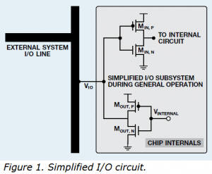 The pin in Figure 1 connects to a multiplexed node, with its operation set by a verified system architecture. As an I/O pin, it has both input and output functions.
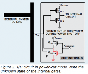
Disregarding issues with the device used for the power switch, turning off the supply for this chip (assuming that none of the chip operations are required) would lead to the situation shown in Figure 2, with unknown states scattered throughout the chip core. In the worst case, the floating gate output devices (MOUT, p and MOUT, n) could be exposed to unexpected external voltages while they are electrically asleep. With a complementary metal-oxide semiconductor (CMOS) I/O, as shown in this example, this could lead to a low-impedance connection to ground via the drain connection of the n-type metal oxide semiconductor (NMOS), highlighted in red. A high current would ensue, possibly maxing out the drive capacity of the previous stage, causing damage to the MOS circuit in the chip, or both. If it did not damage the system, it could still decrease its performance.
Power-down mode
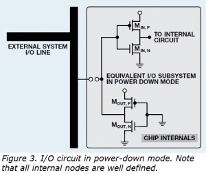
Power-down modes equip the chip with an extra layer of protection against these undesired operating conditions. The implementation differs for different modes, product families and vendors, but the essential focus is on providing a safe I/O boundary while the core of the chip sleeps, maintaining a known, dependable and low-power state. The advantage is that I/O operations between system components, with a system-wide multiplexed bus, for example, do not pose a threat to the sleeping device. One implementation could put the I/O pins in a high-impedance state during low-power mode, allowing the internal nodes connecting to the boundary pin to be in a well-defined state. A simplified implementation is shown in Figure 3. Signals will have no impact on the internal circuit, keeping them intrinsically safe. Other implementations, such as light-sleep modes might keep the I/O periphery powered up as well, while ensuring that the interaction between the chip’s peripherals and core are verified during power-down mode. This enables the chip to handle active use situations, while keeping power consumption low. In addition, this system reduces the cost of the power switch, which would otherwise need to be a large, low-resistance device that would consume significant leakage and on-state power.
Power-down modes vary from chip to chip and vendor to vendor, so names such as “light-sleep mode” might not always mean the same thing. Some of these enable memory retention, while others might permit an increased number of interrupts or other similar features. One prominent advantage of these modes is reduced system response time, as compared to full-power shutdown. Some circuits provide separate I/O and core supplies. One advantage of this decoupling is that the board designer can shut off the core supplies to reduce leakage, while keeping the I/O powered. It is always advisable to get the exact details from the data sheet to ensure that the required features and protection methods are supported.


