

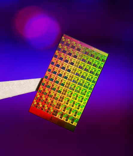
The ‘chips’ are everywhere today, right from mobile phones and computers to microwave ovens and washing machines, and even in children’s toys. There are millions of chips in the world and more are being produced every day, but did you know that these are still produced by a countable number of manufacturers across the world? A fab, or a semiconductor manufacturing plant, is a technology- and resource-intensive factory that could cost anywhere between 1 billion and 10 billion dollars, or even more to set up.
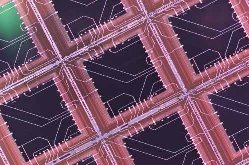
The challenges and resulting improvements in semiconductor fabrication technology can be attributed to the complexity and sensitivity of the whole process. It could take six to eight weeks per batch right from wafer processing and die preparation to integrated circuit packaging and testing. What’s more, it is a very sensitive process too. As chips get smaller, purer materials are sought. The ‘clean rooms’ of fabs, where most of the processes happen, need to be cleaner than you can imagine. Human workers need to wear special suits so that chips do not get contaminated. High-precision machines are needed because working is required at the micrometre and nanometre scale with very sensitive materials.

As the industry transitioned from micro- to nanometre scales, the onus was on the fabs to execute the engineer’s dreams, and they did. Now even 40nm and 30nm technologies have entered the mainstream and smaller feature sizes are on the anvil. Technologies such as three-dimensional integrated circuits (3D ICs) are promis-ing a dramatic reduction in the size of chips in this decade, while research in the field of carbon nanotubes is indicating the arrival of a revolution as innovations continue to fire our dreams.
However, Pankaj Sathe, executive director and head of the Semiconductor Solutions Group, KPIT Cummins, provides a very practical perspective. He says, “The trend towards lower geometries and faster transistors has somewhat slowed down. In an effort to keep pace, parallel computing is evolving. It is expected that even embedded devices will have more than 60 microprocessor cores by 2015. And, since speed is no longer the main differentiator, improvement in manufacturing technologies are no longer sought after so much, as in the past. However, yield improvement technologies are gaining traction in the physical design space.”
This is not to be misconstrued as a reduction in the amount of innovation in the space. It is just that the goals are changing. Today, researchers are working to address immediate concerns such as yield improvement, power management, cost and time-to-market, while also looking at futuristic options such as carbon nanotubes.
There have been significant developments in recent times. Listing some examples, Professor Srikanth Jadcherla, chairman and CEO, Seer Akademi, says, “Kingston has developed what it claims to be the fastest Intel-certified memory in the world, which runs at 2400 MHz. Samsung has announced that it is now shipping 32GB NAND memory chips using 30nm technology, allowing to double the capacity of Samsung’s previous generation. 45.72cm (18-inch) wafer prototypes are being talked about.”
Sathe adds more examples such as the mainstream adoption of 40nm manufacturing technology that is helping some semiconductor sectors improve manufacturing margins and the adoption of the fab-lite model that is helping in removing manufacturing volatility.
Let us take a look at some of these developments.
Chips in 3d
3D IC technology appears to be a greatly discussed development in the semiconductor fabrication world. In a 3D IC, two or more layers of active electronic components are integrated both vertically and horizontally into a single circuit. There are many types of 3D ICs and many techniques for making them. One futuristic option is a completely monolithic 3D chip that is fabricated on a single semiconductor wafer. As of now, the 3D options include wafer-on-wafer, die-on-wafer or die-on-die layering with some form of interconnection.
Flipped chips. Few basic forms of layering have been done for some time now—here, one chip is flipped on top of another and attached at specific bonding areas where micro-bumps are grown to create die-die interconnects. Digital camera chips often use this technology to attach the charge-coupled-device image sensor to the image-processing chip. The technique can also be used to put a memory chip on top of a logic chip, as in the case of Apple’s A4 chip. Industry-wide initiatives are on to standardise the pattern of micro-bumps to use for flipping dynamic random-access memory (DRAM) units atop processor chips. However, this type of flipping actually involves two separate chips, and cannot really be considered a 3D IC.


