Here’s a low-cost DC to DC converter circuit that converts 6V DC into 12V DC. It uses no transformer and is easy to construct with few components.
The circuit is built around IC 555, which generates the required frequency of around 2 to 10 kHz to drive power transistor BD139 (T2). The output frequency of the IC can be adjusted by a 47k potmeter (VR1) and given to the base of transistor T2 via resistor R3. Transistor T2 is mounted on an aluminium heat-sink. Inductor L1 and capacitor C5 (2200µF, 35V) are energy storage components. The 12V zener diode regulates the voltage across the output of the circuit.
DC To DC Converter circuit Diagram
The inductor comprises 100 turns of 24SWG enameled copper wire wound on a 40mm dia. toroidal ferrite core. The more the turns on the core, the higher the current delivering capability of the circuit to the load at the output.
The output current is controlled by transistor BC549 (T1) with the help of resistors R4 and R5. The output voltage is controlled by the zener diode and smoothed by capacitor C5.
You can obtain regulated 12V DC, 120 mA across the output of this circuit. At higher loads (below 100 ohms), the circuit might not perform well and deliver as much current. Use a large capacitor (C5) and inductor for higher voltages and higher currents, respectively. Different output voltages can be obtained by using zener diodes of other ratings.
FM transmissions can be received within a range of 40 km. If you are in fringe areas, you may get a very weak signal. FM DXing refers to hearing distant stations (1500 km or more) on the FM band (88-108 MHz). The term ‘DX’ is borrowed from amateur radio operators. It means ‘distance unknown’; ‘D’ stands for ‘distance’ and ‘X’ stands for ‘unknown.’ For an FM receiver lacking gain, or having a poor signal-to-noise ratio, using an external preamplifier improves the signal level. The dual-gate MOSFET based preamplifier circuit shown in Fig. 1 gives an excellent gain of about 18 dB. It costs less and is simple to design.
Field effect transistors
Field-effect transistors (FETs) are superior to bipolar transistors in many applications as these have a much higher gain—approaching that of a vacuum tube. These are classified into junction FETs and MOSFETs. On comparing the FETs with a vacuum tube, the gate implies the grid, the source implies the cathode, and the drain implies the plate. In a transistor, the base implies the grid, the emitter implies the source, and the collector implies the drain.
In dual-gate FETs, gate 1 is the signal gate and gate 2 is the control gate. The gates are effectively in series, making it easy to control the dynamic range of the device by varying the bias on gate 2. The MOSFET is more flexible because it can be controlled by a positive or negative voltage at gate 2. The resistance between the gate and rest of the device is extremely high because these are separated by a thin dielectric layer. Thus the MOSFET has an extremely high input impedance.
Dual Gate MOSFETs
Dual-gate MOSFETs (DG MOSFETs) are very popular among radio amateurs. These are being used in IF amplifiers, mixers, and preamplifiers in HF-VHF transceivers. The isolation between the gates (G1 and G2) is relatively high in mixer applications. This reduces oscillator pulling and radiation. The oscillator pulling is troublesome particularly in shortwave communications. It is a characteristic in many unsophisticated frequency-changer stages, where the incoming signal, if large, pulls the oscillator frequency slightly off the frequency set by the tuning knob and towards a frequency favourable to the (large) incoming signal.
A DG MOSFET can also be used for automatic gain control in RF amplifiers.
MOSFET based preamplifier circuit operation
DG MOSFET BF966S is an n-channel depletion-type MOSFET that is used for general-purpose FM and VHF applications. In this configuration, it is used for FM radio band. The quadratic input characteristic of the FET input stage gives better results than the exponential characteristic of a bipolar transistor. Gate 1 is meant for input and gate 2 is for gain control. The input from the antenna is fed to gate G1 via C1 and L1. Trimmer VC1 is used to tune and select the input frequencies. Capacitor C4 (100 kpF) at the gain control electrode (gate 2) decouples any variation in G2 voltage at radio frequencies to maintain constant gain. Set preset VR (47k) to adjust the gain or connect a fixed resistor for fixed gain.
The output of the circuit is obtained via capacitor C5 and fed to the FM receiver amplifier.For indoor use, connect a ¼-wavelength whip antenna, ½-wavelength 1.5m wire antenna, or any other indoor antenna set-up with this circuit. You may use a 9V battery without the transformer and diode 1N4007, or any 6V-12V power supply to power the circuit (refer Fig. 1). The RF output can be taken directly through capacitor C5. For an improved input and output impedance, change C1 from 1 kpF to 22 pF and C5 from 1 kpF to 100 kpF.
Fig. 1: Circuit of MOSFET-based preamplifier for FM DXing
Setting up the system
For outdoor use at top mast, like a TV booster, connect the C5 output to the power supply unit (PSU) line. Use RG58U/RG11 or RG174 cable for feeding the power supply to the receiver amplifier. The PSU for the circuit is the same as that of a TV booster. For TV boosters, two types of mountings are employed: The fixed tuned booster is mounted on the mast of the antenna. The tunable booster consisting of the PSU is placed near the TV set for gain control of various TV channels. (For details, refer ‘High-Gain 4-Stage TV Booster’ on page 72 of Electronics Projects Vol. 8.)
Mount the DG MOSFET BF966S at the solder side of the PCB to keep parasitic capacitance as small as possible. Use an epoxy PCB. After soldering, clean the PCB with isopropyl alcohol. Use a suitable enclosure for the circuit. All component leads must be small. Avoid shambled wiring to prevent poor gain or self oscillations. Connecting a single-element cubical quad antenna to the circuit results in ‘Open Sesam’ for DXing.
Here is a simple non-contact AC power monitor for home appliances and laboratory equipment that should remain continuously switched-on. A fusefailure or power breakdown in the equipment going unnoticed may cause irreparable loss. The monitor sounds an alarm on detecting power failure to the equipment.
The circuit is built around CMOS IC CD4011 utilising only a few components. NAND gates N1 and N2 of the IC are wired as an oscillator that drives a piezobuzzer directly. Resistors R2 and R3 and capacitor C2 are the oscillator components. The amplifier comprising transistors T1 and T2 disables the oscillator when mains power is available.
In the standby mode, the base of T1 picks up 50Hz mains hum during the positive half cycles of AC and T1 conducts. This provides base current to T2 and it also conducts, pulling the collector to ground potential.
As the collectors of T1 and T2 are connected to pin 2 of NAND gate N1 of the oscillator, the oscillator gets disabled when the transistors conduct. Capacitor C1 prevents rise of the collector voltage of T2 again during the negative half cycles. When the power fails, the electrical field around the equipment’s wiring ceases and T1 and T2 turn off. Capacitor C1 starts charging via R1 and preset VR and when it gets sufficiently charged, the oscillator is enabled and the piezobuzzer produces a shrill tone. Resistor R1 protects T2 from short circuit if VR is adjusted to zero resistance.
The circuit can be easily assembled on a perforated breadboard. Use a small plastic case to enclose the circuit and a telescopic antenna as aerial. A 9V battery can be used to power the circuit. Since the circuit draws only a few microamperes current in the standby mode, the battery will last several months. After assembling the circuit, take the aerial near the mains cable and adjust VR until the alarm stops to indicate the standby mode. The circuit can be placed on the equipment to be monitored close to the mains cable.
Most optical interruption counters make use of a light bulb with light-dependent resistor (LDR) or ordinary phototransistor as the sensor. The interruption counter work satisfactorily in darkness only and cannot be used outdoors because of the chances of false counting due to light sensed from other light sources like sun, light bulb, etc.
Infrared interruption counter
The interruption counter described here uses an infrared (IR) sensor that can sense a particular modulated frequency of infrared beam. A small transmitter circuit employing an IR LED is used to emit modulated IR signals.
Fig. 1: Block diagram of infrared interruption counterFig. 2: Power supply circuitFig. 3: IR transmitter circuit
The block diagram of the infrared interruption counter providing an overview of the system is shown in Fig. 1. The astablemultivibrator produces 36kHz frequency and npn transistor BC547 drives the IR LED to transmit the modulated infrared signal. The transmitted IR signal continuously falls on the IR sensor (receiver).
When somebody crosses the path of the IR beam falling on the sensor, the triggering circuit activates to trigger the monostable multivibrator. The output of the monostable advances the count of the 4-digit counter-cum-display driver to display the count on 7-segment, common-cathode displays.
Circuit description
The infrared interruption counter circuit consists of power supply, transmitter and infrared interruption counter stages.
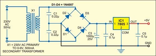
Power supply
Fig. 2 shows the power supply circuit. The AC mains is stepped down by transformer X1 to deliver secondary output of 9V at 500 mA. The transformer output is rectified by a full-wave bridge rectifier comprising diodes D1 through D4, filtered by capacitors C3 and C4, and regulated by IC 7805 (IC1) to provide regulated 5V supply for the transmitter and infrared receiver-cum-counter stages. Capacitor C5 bypasses any ripple in the regulated output.
Transmitter stage
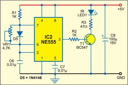
The transmitter circuit (see Fig. 3) works off 5V regulated supply. It is built around timer NE555 (IC2), npn transistor BC547, IR LED1 and some resistors and capacitors.
Fig. 4: Circuit of infrared interruption counter
Timer NE555 is wired as an astable multivibrator whose frequency is set at 36 kHz by adjusting preset VR1. The npn transistor (T1) is used to drive IR LED1, which can transmit modulated IR signals up to around 7 metres without any lense arrangement.
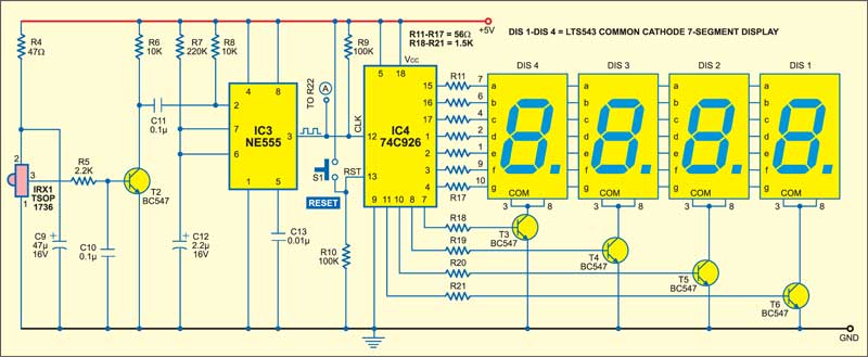
Infrared interruption counter stage. The IR interruption counter circuit (Fig. 4) is built around IR receiver TSOP1736 (IRX1) utilising timer NE555 (IC3), 4-digit counter-cum-display driver IC 74C926 with multiplexed 7-segment output drivers (IC4), 7-segment common-cathode displays DIS1 through DIS4, BC547 npn transistors and some discrete components.
Fig. 5: Internal pin configuration of IC 74C926Fig. 6: Audible beeper (optional)
IR sensor TSOP1736 is readily available in the market. It is commonly used in TV sets as a miniaturised receiver for IR remote control systems. Fig. 5 shows the internal functional block diagram and pin configuration of IC 74C926.
IR receiver module TSOP 1736 is meant for pulsed operation. When it is exposed to continuous 36kHz modulated IR beam, its output remains high and the collector of transistor T2 is held low. During a brief interruption of the IR beam, a low-to-high-to-low pulse appears at the collector of transistor T2 to trigger the monostable formed by IC3. The monostable multivibrator is set for a time delay of nearly half second. The 4-digit counter with multiplexed 7-segment output drivers (IC 74C926) advances by one digit for every clock pulse received from the multivibrator. It can count up to ‘9999.’ The counter can be reset to zero at any time by pressing the reset microswitch.
Thus the display, at any time, shows the count of interruption of the IR beam since the last reset. The interruption counter can be employed as visitor counter or object counter in industrial applications.
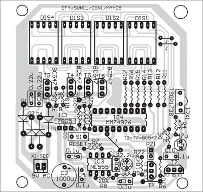
Fig. 7: Single-side PCB for IR transmitterFig. 8: Components layout for the PCB in Fig. 7
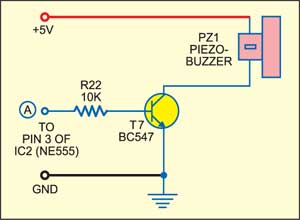
You can add a beeper circuit, as shown in Fig. 6, to provide an audible indication of each interruption. The output pulse from monostable IC3, generated during an interruption, will activate transistor T7 to drive the piezobuzzer for duration of the monostable pulse.
Construction
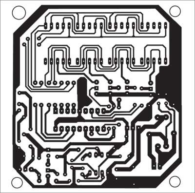
A single-side PCB layout for the IR transmitter (Fig. 3) is shown in Fig. 7 and its components layout in Fig. 8, while the combined PCB layout for the interruption counter (Fig. 4), power supply (Fig. 2) and beeper (Fig. 6) is shown in Fig. 9 with its components layout in Fig. 10.
Fig. 9: Single-side combined PCB layout for infrared interruption counter, power supply and beeperFig. 10: Components layout for the PCB in Fig. 9
For easy servicing, use IC bases to mount the ICs on the PCB. After assembling the PCB, place it near the entry gate. Use long wires for connections to the IR transmitter LED and IR receiver TSOP1736 so that these can be taken out of the PCB and mounted on the opposite pillars of the entry gate. The transmitter should be oriented such that the transmitted IR ray directly falls on the receiver module.
The article was first published in September 2005 and has recently been updated.
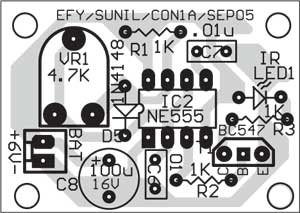
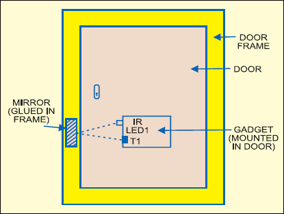
If some intruder tries to open the door of your house, this circuit sounds an alarm to alert you against the attempted intrusion.
The circuit (Fig. 1) uses readily available, low-cost components. For compactness, an alkaline 12V battery is used for powering the unit. Input DC supply is further regulated to a steady DC voltage of 5V by 3-pin regulator IC 7805 (IC2).
Fig. 1: Circuit of the door guard
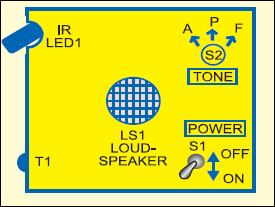
Assemble the unit on a general-purpose PCB as shown in Fig. 4 and mount the same on the door as shown in Fig. 3. Now mount a piece of mirror on the door frame such that it is exactly aligned with the unit. Pin configurations of IC UM3561 and transistors 2N5777 and BC547 are shown in Fig. 2.
Fig. 2: Pin configurations of UM3561 and transistors 2N5777 and BC547
Initially, when the door is closed, the infrared (IR) beam transmitted by IR LED1 is reflected (by the mirror) back to phototransistor 2N5777 (T1). The IR beam falling on phototransistor T1 reverse biases npn transistor T2 and IC1 does not get positive supply at its pin 5. As a result, no tone is produced at its output pin 3 and the loudspeaker remains silent. Resistor R1 limits the operating current for the IR LED.
When the door isopened, the absence of IR rays at phototransistor T1 forward biases npn transistor T2, which provides supply to positiveIC1. Now 3-sirensound generator IC UM3561 (IC1) gets power via resistor R5. The output of IC1 at pin 3 is amplified by Darlington-pair transistors T3 and T4 to produce the alert tone via the loudspeaker.
Fig. 3: Back view of the door assembly
Rotary switch S2 is used to select the three preprogrammed tones of IC1. IC1 produces fire engine, police and ambulance siren sounds when its pin 6 is connected to point F, P or A, respectively.
Fig. 4: Suggested enclosure with major components layout
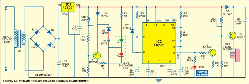
This circuit gives audio-visual indication of the failure and resumption of mains power. The circuit is built around dual timer IC LM556. When mains is present the bicolour LED glows in green colour, and when mains fails it turns red.
The AC mains is stepped down by transformer X1 to deliver the secondary output of 12V at 250 mA. The transformer output is rectified by a full-wave bridge rectifier comprising diodes D1 through D4, filtered by capacitor C1 and regulated by IC 7809 (IC1) to give regulated 9V DC to operate the circuit.
9V battery and pnp transistor T1 have been used here as the power source for red light indication of the absence of power. Transistor T1 can be made to conduct or cut-off easily by varying preset VR1.
Power Failure And Resumption Alarm Circuit
Initially, when mains is present, pnp transistor T1 is in cut-off state and therefore bicolour LED1 glows in green colour.
When power fails, pnp transistor T1 starts conducting and bicolour LED1 glows in red colour. Due to non-availability of Vcc voltage at pin 14 of IC2, its output pin 9 remains low and transistor T3 does not conduct. However, capacitor C7 (4700µF) holds adequate charge and hence transistor T4 conducts and piezobuzzer PZ1 sounds continuously for around eleven seconds until capacitor C7 discharges completely.
When power resumes, bicolour LED1 glows in green colour and the buzzer beeps for around 14 seconds.
Dual timer IC LM556 (IC2) sections have been used here in monostable and astable modes, respectively.
In the monostable section, location of the external timing capacitor determines whether a positive or negative output pulse is generated. Diode D7 ensures that even a momentary power loss will cause a pulse to be generated when the power resumes. With capacitor C3 connected to ground, a positive output pulse is generated according to the following relationship:
T = 1.1×R5×C3.
This positive output is present at pin 5 of IC2. Since IC2 is a dual-timer IC, its first output is directly fed to reset pin 10 of second section. Therefore the second timer of IC2 starts oscillating. Its frequency of oscillations (F0) is determined by resistors R6 and R11 and capacitor C6 as follows:
F0=1.4/(R6+2R11)×C6.
IC LM556 outputs frequencies in the form of pulses at its pin 9. These pulses are coupled to npn transistor T3, which conducts and cuts off depending on the output at pin 9 of IC2. Red LED2 is connected to pin 9 via current-limiting resistor R7 (270-ohm) to indicate power resumption.
The collector output of transistor T3 is directly fed to the base of pnp transistor T4, due to which base biasing of T4 varies and the buzzer beeps for around 14 seconds.
For reading other interesting Electronics projects: click here
This Solar Bug circuit takes power from a small solar panel and then produces a sound in a buzzer momentarily when the relaxation oscillator signal passes through it.
Hide this solar powered circuit suitably and see the reaction of your friends to the chirpy sound produced by it every few minutes. In all probability, it will coax them to find out where the sound is coming from.
The circuit runs off a miniature solar power panel, which can be taken out from an old calculator such as Citizen CT-500. A panel giving 1.5V to 2.5V is required. Note that the circuit can work properly from a panel as small as 3 cm2.
If a digital voltmeter is connected across capacitor C2, a slow build-up of voltage can be observed when the panel is exposed to light. Transistors T1 and T2 form a relaxation oscillator. When C1 charges to 0.6V, transistor T1 conducts and the charge built up in C2 is discharged through the piezobuzzer to produce a short beep.
While testing the circuit, the value of resistor R1 can be reduced to, say, 1 kilo-ohm. Use a good-quality buzzer to ensure that the sound produced is loud enough.
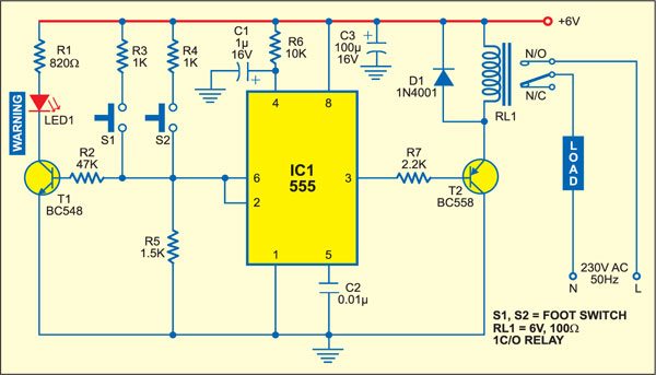
Certain industrial controls require accurate switching operations. For example, in case of a foot-switch for precise drilling work, even a small error in switching may cause considerable loss. This low-cost but accurate foot-operated switch can prevent that.
IC NE555 is wired in one-shot mode. Its output pin 3 goes high only when both switches S1 and S2 are pressed simultaneously. You can release any one of the switches without changing the output state. When you release both the switches, the output goes low.
Fig. 1: Circuit of the foot-switch
The switches are placed under a foot paddle as shown in Fig. 2. LED1 is used as a warning indicator. If either S1 or S2 gets pressed erroneously, LED1 blinks to warn the operator. The operator can then withdraw his foot in case of a mistake or depress the other switch also to trigger the circuit. LED1 is to be mounted on the operator’s desk.
The circuit operation is simple. Resistors R2, R3 and R4 form a voltage divider. IC NE555 has two comparators, a flip-flop and power output section built into it. Pressing either S1 or S2 puts the input voltage between the upper comparator (2/3Vcc) and the lower comparator (1/3Vcc). Thus, it has no effect on the state of the internal flip-flop of IC NE555. Pressing the two switches simultaneously sets the flip-flop and the output of NE555 goes high. Transistor T2 energises relay RL1 for driving the load.
Fig. 2: Foot paddle switch
Releasing any of the switches brings the comparator voltage back to the initial level inside NE555 and it has no effect on the state of the flip-flop. Releasing both the switches brings the input level with respect to ground below the low trigger level, and thus it resets the output.
Use of the voltage divider results in stable operation over the entire permissible supply voltage range. The RC circuit at pin 4 provides power-on reset.
When only S1 is pressed, R3 (1 kilo-ohm) is less than R5 (1.5 kilo-ohms) and IC1 is not triggered. However, transistor T1 (BC548) gets forward biased and LED1 glows. When both S1 and S2 are pressed, the effective resistance between +Vcc and pin 2 of IC1 is about 500 ohms, which is less than R5 (1.5 kilo-ohms), and IC NE555 gets triggered.
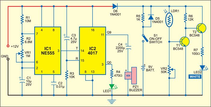
Many a times equipment at workstations remain switched on unnoticed. In this situation, these may get damaged due to overheating. Here is an add-on device for the workbench power supply that reminds you of the power-on status of the connected devices every hour or so by sounding a buzzer for around 20 seconds. It also has a white LED that provides good enough light to locate objects when mains fails.
Fig. 1: Circuit of power-on reminder with LED lamp
Fig. 1 shows the circuit of power-on reminder with LED lamp. Here, IC NE555 (IC1) is wired as an astable multivibrator, whose time period is set to around six minutes using resistors R1 and R2, preset VR1 and capacitor C1 for sounding the buzzer every hour. The output of IC1 is fed to the clock input of IC CD4017 (IC2). Capacitor C3 and resistor R3 provide power-on-reset pulse to IC2.
When power to the circuit is switched on, pin 3 of IC2 goes high. After around one hour, its output pin 11 (Q9) goes high and the buzzer sounds. This cycle repeats until the two npn transistors. The LDR offers a very high resistance in darkness, i.e., when no light falls on it. Therefore when power fails, transistor T1 gets reverse biased to drive transistor T2 and the white LED (LED2) glows. The lamp circuit is powered by a 9V rechargeable battery, which is charged via resistor R5 when mains is present. Thus in darkness, the LED remains power to the circuit is switched off.
Fig. 2: Power supply circuit
The automatic lamp is built around a light-dependent resistor (LDR) and ‘on.’
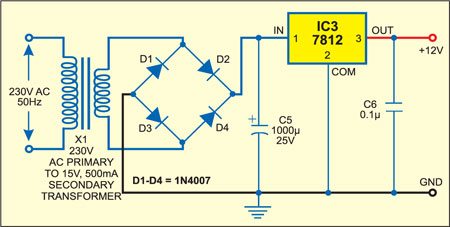
Fig. 2 shows the power supply circuit. The AC mains is stepped down by transformer X1 to deliver a secondary output of 15V AC at 500 mA. The transformer output is rectified by a bridge rectifier comprising diodes D1 through D4, filtered by capacitor C5 and regulated by IC 7812 (IC3) to provide regulated 12V to the circuit. Capacitor C6 bypasses any ripple in the regulated output.
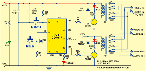
Need to connect more than one audio-video (AV) source to your colour television? Don’t worry, here’s an AV input expander for your TV. It is inexpensive and easy to construct.
The working of the circuit is simple and straightforward. Whenever 12V DC is applied to the circuit, power-on LED1 glows. Now reset the decade counter by momentarily pressing switch S2 to make Q0 output of IC1 high. LED2 glows to indicate that the circuit is ready to work.Switch S1 is used for selecting a particular audio-video (AV) signal. To select the first AV signal, press switch S1 once. To select the second AV signal, press switch S1 twice. In the same way, you can select the other two signals.
Momentarily pressing of switch S1 once results in clocking of the decade counter and relay driver transistor T1 conducts to energise relay RL1. Now normally opened (N/O) contacts of two-changeover relay RL1 connect the television set’s inputs to the first AV signal (marked as Video-In 1 and Audio-in 1). LED3 glows to indicate this.
When you press switch S1 twice, the Q2 output of IC1 goes high. Consequently, 2C/O relay RL2 (not shown in the circuit) energises and television inputs are connected to the second AV signal (not shown in the figure). LED4 (not shown in figure) glows to indicate this.
Similarly, pressing switch S1 thrice makes the Q3 output of IC1 high. Consequently, 2C/O relay RL3 (not shown in the figure) energises and the television inputs are connected to the third AV signal source. LED5 (not shown in the figure) glows to indicate this. Again, pressing switch S1 four times makes the Q4 output of IC1 high. Consequently, 2C/O relay RL4 energises and the TV inputs are connected to the fourth AV signal source (marked as Video-in 4 and Audio-in 4). LED6 glows to indicate this.
Further pressing of switch S1 resets the decade counter and LED2 glows again. Thereafter, the cycle repeats. The circuit is wired for four-input selection, therefore the Q5 output of IC1 is connected to reset pin 15 of IC1.
Enclose the assembled PCB along with the relays in a cabinet with the input/output sockets and indicators mounted on the body of the cabinet.


 Here’s a low-cost DC to DC converter circuit that converts 6V DC into 12V DC. It uses no transformer and is easy to construct with few components.
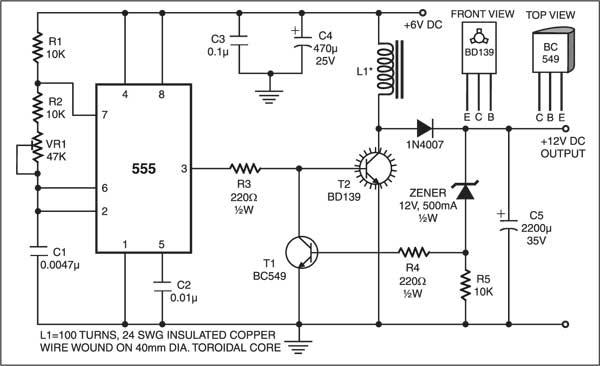

 FM transmissions can be received within a range of 40 km. If you are in fringe areas, you may get a very weak signal. FM DXing refers to hearing distant stations (1500 km or more) on the FM band (88-108 MHz). The term ‘DX’ is borrowed from amateur radio operators. It means ‘distance unknown’; ‘D’ stands for ‘distance’ and ‘X’ stands for ‘unknown.’ For an FM receiver lacking gain, or having a poor signal-to-noise ratio, using an external preamplifier improves the signal level. The dual-gate MOSFET based preamplifier circuit shown in Fig. 1 gives an excellent gain of about 18 dB. It costs less and is simple to design.
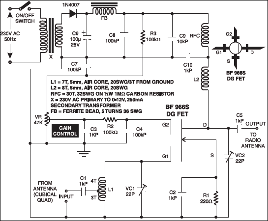

 Here is a simple non-contact AC power monitor for home appliances and laboratory equipment that should remain continuously switched-on. A fusefailure or power breakdown in the equipment going unnoticed may cause irreparable loss. The monitor sounds an alarm on detecting power failure to the equipment.
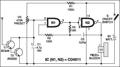

 Most optical interruption counters make use of a light bulb with
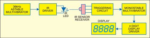


 If some intruder tries to open the door of your house, this circuit sounds an alarm to alert you against the attempted intrusion.
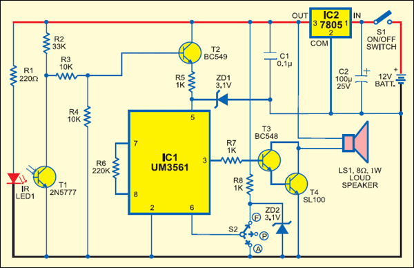


 This Solar Bug circuit takes power from a small solar panel and then produces a sound in a buzzer momentarily when the relaxation oscillator signal passes through it.
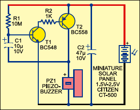


 Many a times equipment at workstations remain switched on unnoticed. In this situation, these may get damaged due to overheating. Here is an add-on device for the workbench power supply that reminds you of the power-on status of the connected devices every hour or so by sounding a buzzer for around 20 seconds. It also has a white LED that provides good enough light to locate objects when mains fails.