




EDGE INSPECT: An AI-Based PCB Missing Component Detection System on Arduino UNO Q is an edge-AI inspection solution designed to automate the verification of assembled printed circuit boards (PCBs) by identifying missing, misplaced, and unexpected components. The system uses a camera to capture an image of a populated PCB and processes it using a YOLO-based object-detection model running on the Arduino UNO Q platform. By combining visual inspection with electronic design and manufacturing data, EDGE INSPECT aims to improve assembly quality, reduce manual inspection effort, and identify component-placement defects at an early stage.
The proposed system compares detected components and their positions against the expected board configuration derived from the Bill of Materials (BOM), Pick-and-Place data, and Gerber design files. The inspection pipeline identifies expected components that are missing, detects components placed outside their intended locations, and flags unexpected components that do not match the reference design. Based on the comparison, the system generates a clear PASS or FAIL result accompanied by a detailed list of detected discrepancies. Processing at the edge enables local inspection and reduces dependence on cloud-based image analysis.
By integrating computer vision, design-data comparison, and automated quality reporting, EDGE INSPECT provides a foundation for accessible, AI-assisted PCB assembly inspection in electronics laboratories, prototyping facilities, and small-scale manufacturing environments. The system’s effectiveness depends on accurate component detection, reliable alignment between PCB images and design coordinates, and appropriate handling of component orientation and visually similar packages. Validation across different PCB layouts, component sizes, lighting conditions, and assembly defects is necessary to establish inspection accuracy and suitability for production use.
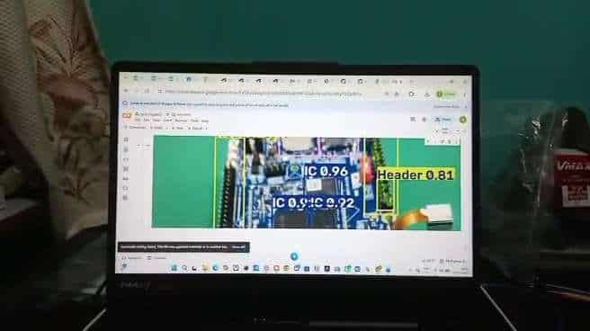
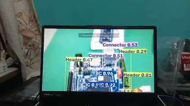
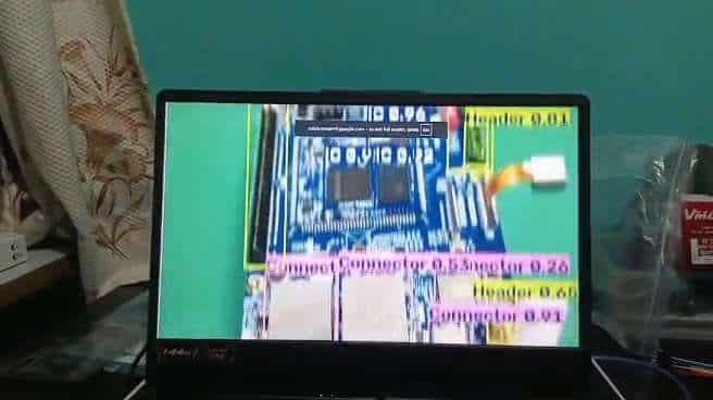
The video shows the trained YOLO model running on live camera footage of a development board. Bounding boxes with class names and confidence scores appear in real time: IC (0.96, 0.92), Header (0.81, 0.47, 0.29), and Connector (0.53, 0.51, 0.91). Frames taken from the video are shown below.
Component List
| ID | Name | Designator | Quantity | Purpose |
|---|---|---|---|---|
| 1 | Arduino UNO Q (Qualcomm QRB2210 MPU + STM32U585 MCU) | MOD1 | 1 | Main edge-computing platform: runs Linux, Python, FastAPI and AI inference (MPU) and hardware control (MCU) |
| 2 | Smartphone camera (Wi-Fi connected) | CAM1 | 1 | Captures the PCB photograph (initial prototype); later USB/CSI/industrial camera |
| 3 | PCB under inspection (assembled board) | PCB1 | 1 | Device under test |
| 4 | Computer / laptop | PC1 | 1 | Development, dataset preparation, YOLO training, backend testing |
| 5 | USB-C cable and 5 V supply | CBL1 | 1 | Powers and programs the UNO Q |
| 6 | Wi-Fi network | NET1 | 1 | Phone ↔ backend communication (HTTP / REST) |
Software components: Python, FastAPI, Uvicorn, YOLOv8 (Ultralytics), OpenCV, HTML/CSS/JavaScript (mobile interface), Arduino App Lab, Arduino sketch (C/C++) for the STM32 side.
Project Explanation Step By Step
Problem Statement
After a PCB is assembled, components can be left out (missing), soldered at the wrong place (misplaced), or fitted where nothing was designed (unexpected). Manual visual inspection is slow, tiring, inconsistent and depends on the operator. Commercial automated optical inspection (AOI) machines are accurate but expensive and not affordable for students, small workshops and start-ups. There is a need for a low-cost, portable, easy-to-use inspection tool.
Objective
The main objective of PCB-INSPECTOR is to automatically inspect an assembled PCB and identify:
- Missing components – expected by the design but not found on the board.
- Misplaced components – found, but at a wrong position.
- Unexpected components – found where no component is expected.
- Incorrect component placement – wrong location or orientation compared with the design.
Proposed Solution
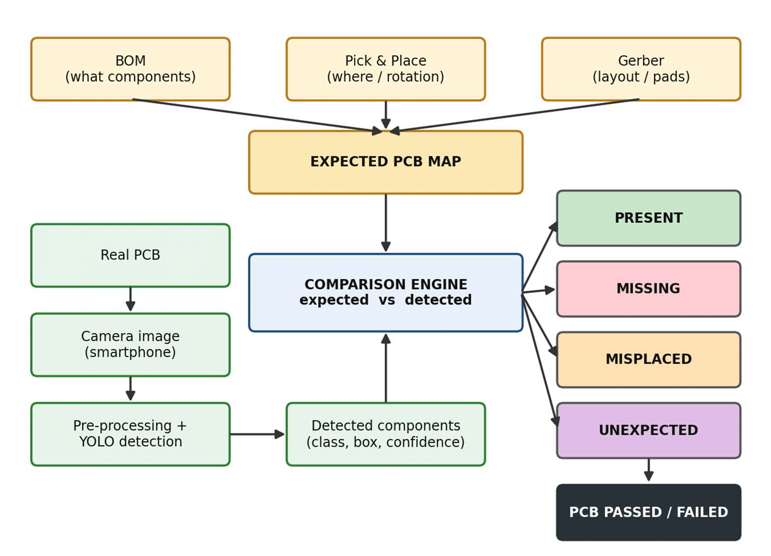
PCB-INSPECTOR compares what the PCB should look like with what it actually looks like. The “should” comes from the design files (BOM, Pick & Place, Gerber). The “actually” comes from a camera photo analysed by an AI object-detection model. A comparison engine matches the two and produces a clear PASS/FAIL report. The heavy processing is designed to run at the edge on an Arduino UNO Q, so the system is compact, works offline and does not depend on cloud services.
Step-by-Step Working
Step 1 – Prepare the expected PCB map from the design data
Three design files describe the correct board:
| Input | What it tells the system | Example |
|---|---|---|
| BOM (Bill of Materials) | WHAT components must be present | R1 – Resistor, C1 – Capacitor, U1 – IC, LED1 – LED |
| Pick & Place (P&P) | WHERE each component must be (X, Y, rotation) | R1 → X 25.2, Y 14.5; C1 → X 30.1, Y 20.2; U1 → X 45.0, Y 30.2 |
| Gerber files | Physical layout: copper layers, pads, tracks, solder mask, silkscreen, board outline – gives the coordinate reference | Board outline and pad positions |
Combining BOM + P&P + Gerber gives the EXPECTED PCB MAP – a list of every component that should exist and its exact location on the board.
Step 2 – Capture the real PCB image
The user presses SCAN PCB on the mobile interface; the phone camera opens and photographs the assembled board (or a photo can be uploaded). In the prototype a smartphone camera is used; later a USB camera, CSI camera or industrial camera can be attached for repeatable, fixed-position imaging.
Step 3 – Pre-process the image and detect components with YOLO
The image is resized and normalised, then passed to a YOLO object-detection model. YOLO (You Only Look Once) finds all objects in one pass, which makes it fast enough for edge devices. For every component it returns a bounding box (location), a class and a confidence score. The model detects general component types:
Resistor, Capacitor, Diode, LED, IC, Connector, Switch/Button, Header, Crystal, Debug/Test point.
Example model output: Capacitor – confidence 0.92 – location X=310, Y=210; IC – confidence 0.95 – location X=450, Y=300.
Important design decision: the AI does not have to read every reference number (such as C17 or R5) from the board. It only needs to say “this is a capacitor at this location”. The BOM + P&P data then say “component C17 (a capacitor) should be at this location”. The comparison engine joins the two, which keeps the AI task simple, robust and accurate.
Step 4 – Compare EXPECTED vs DETECTED (comparison engine)
Detected components are converted to board coordinates and matched to expected components by class and position. The result for each component is one of four categories:
| Result | Meaning | Example |
|---|---|---|
| PRESENT | Expected component found at the expected place | C1, C3, R1, R2, U1 found |
| MISSING | Expected component not found | C2 expected but not detected → MISSING |
| MISPLACED | Component found, but at the wrong position | R1 detected at (400,300) instead of (200,300) |
| UNEXPECTED | Component detected where none is expected | Extra part found at an empty footprint |
Worked example: Expected = C1, C2, C3, R1, R2, U1. Detected = C1, C3, R1, R2, U1. Result: C1 PRESENT, C2 MISSING, C3 PRESENT, R1 PRESENT, R2 PRESENT, U1 PRESENT → PCB FAILED (reason: C2 missing).
Misplacement example: Expected R1 at (200,300) and R2 at (400,300); the camera finds R1 at (400,300) and R2 at (200,300) → both R1 and R2 are reported MISPLACED.
Step 5 – Generate the final PASS / FAIL report
If every expected component is present and correctly placed and nothing unexpected is found, the board is PASSED. Otherwise it is FAILED and the report lists the exact designators. Example final report:
PCB INSPECTION RESULT
---------------------
STATUS:            FAILED
MISSING:           C17
MISPLACED:         R4
UNEXPECTED:        None
TOTAL EXPECTED:    25
TOTAL DETECTED:    24
FINAL:             PCB FAILED
Step 6 – Show the result on the phone
The result (PASS/FAIL, missing, misplaced and unexpected lists, totals) is sent back through the REST API and displayed on the mobile interface so the operator gets an immediate, easy-to-read answer.
Why Arduino UNO Q? (AIoT relevance)
The Arduino UNO Q is a dual-brain board: a Qualcomm QRB2210 microprocessor (MPU) running Linux and an STM32U585 microcontroller (MCU) running Arduino sketches. This is ideal for AIoT:
- MPU (Linux side): runs Python, FastAPI, the YOLO model, image processing and the inspection logic – i.e., the “AI”.
- MCU (STM32 side): runs the Arduino sketch for GPIO and real-time hardware control – i.e., the “IoT / physical” part (e.g., status LEDs, buzzer, reject signal, conveyor or lighting control in future versions).
- Bridge / RPC: lets the Python program on the Linux side call functions on the STM32 side, so AI results can directly trigger hardware actions.
- Edge processing: images are processed locally, giving low latency, privacy and no dependence on internet.
Coding Explanation and Configuration
Development Environment Setup
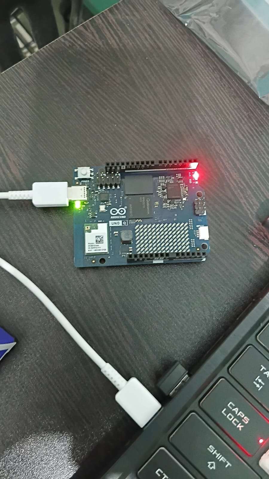
1. Set up the Arduino UNO Q with Arduino App Lab (USB-C connection to the computer, as in Fig 3). Verify the Linux side (Python) and the STM32 side (Arduino sketch) both run, and the Bridge between them works.
2. On the computer install Python and the backend libraries: FastAPI, Uvicorn, Ultralytics (YOLOv8), OpenCV, Pillow, NumPy (listed in requirements.txt).
3. Prepare the dataset and train the model (Section 6.3).
4. Run the backend with Uvicorn and open the mobile interface in the phone browser over Wi-Fi.
Software Structure
PCB-INSPECTOR/
|-- backend/
|   |-- main.py             (FastAPI application)
|   |-- requirements.txt
|   |-- model/detector.py   (loads YOLO model, runs detection)
|   `-- pcb/
|       |-- gerber_parser.py
|       |-- bom_parser.py
|       |-- pnp_parser.py
|       `-- inspection.py   (expected vs detected comparison)
|-- frontend/  index.html  style.css  app.js
|-- unoq/
|   |-- python/main.py      (Linux-side UNO Q app)
|   `-- sketch/sketch.ino   (STM32-side Arduino sketch)
|-- model/README.md
`-- data/ gerber/ bom/ pnp/ test_images/| File | Function |
|---|---|
| backend/main.py | Runs the FastAPI backend and defines the API endpoints |
| model/detector.py | Loads the AI model and performs component detection |
| pcb/gerber_parser.py | Reads Gerber information (layout, board outline) |
| pcb/bom_parser.py | Reads the BOM (which components are required) |
| pcb/pnp_parser.py | Reads Pick & Place data (X, Y, rotation per designator) |
| pcb/inspection.py | Compares expected components with detected components; produces PRESENT / MISSING / MISPLACED / UNEXPECTED and PASS/FAIL |
| frontend/index.html | Creates the mobile interface |
| frontend/style.css | Controls the interface design (dark theme, buttons) |
| frontend/app.js | Camera access, image upload and communication with the backend |
| unoq/python/main.py | Runs the Linux-side UNO Q application |
| unoq/sketch/sketch.ino | Runs the Arduino / STM32 side |
AI Model Training (YOLO)
The detection model is trained with the standard YOLO workflow:
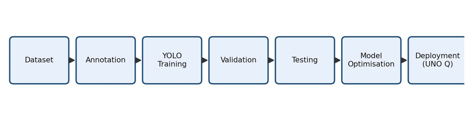
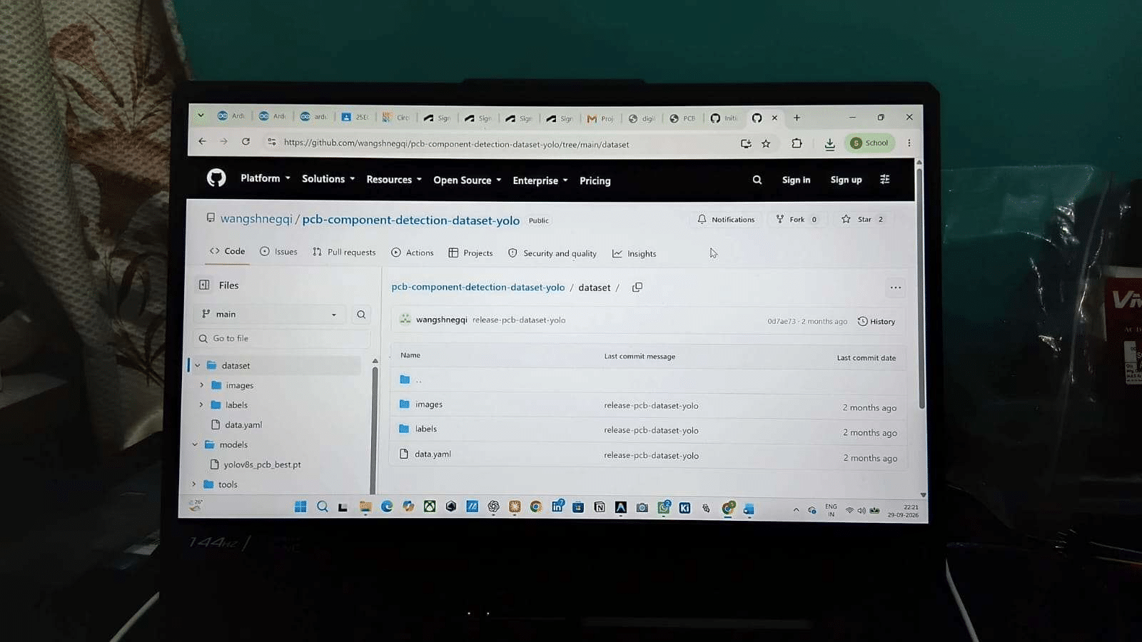
- Dataset: a public PCB component-detection dataset in YOLO format (images/, labels/, data.yaml) was used as the starting point – GitHub repository “wangshnegqi / pcb-component-detection-dataset-yolo”. The repository also contains a YOLOv8-small PCB weights file (yolov8s_pcb_best.pt) and helper tools.
- Annotation: each image has label files with a class and bounding box for every component (Resistor, Capacitor, Diode, LED, IC, Connector, Switch/Button, Header, Crystal, Test point).
- Training & validation: YOLOv8 is trained on the training split and evaluated on the validation split using precision, recall and mAP.
- Testing: the model is tested on unseen PCB photos and on live camera video (Fig 1).
- Optimisation & deployment: the trained weights are optimised/exported for edge inference on the Arduino UNO Q.
Backend – FastAPI Service
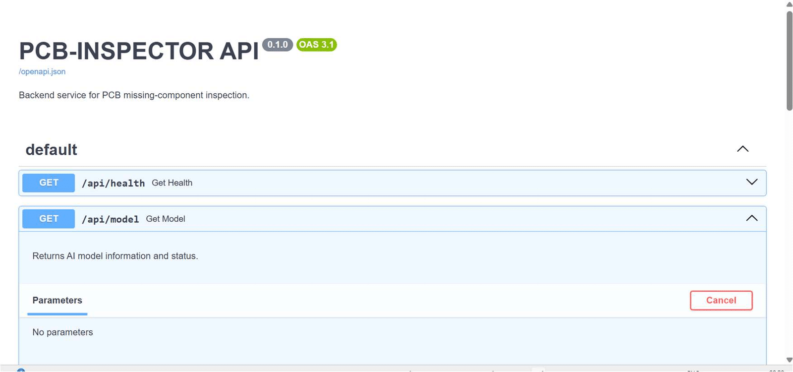
The backend is written in Python with FastAPI and served by Uvicorn. It exposes three endpoints:
| Method | Endpoint | Description |
|---|---|---|
| GET | /api/health | Health check. Expected response: {“status”: “ok”, “service”: “PCB-INSPECTOR”} |
| GET | /api/model | Returns AI model information and status |
| POST | /api/inspect | Receives the PCB image, runs detection and the inspection engine, returns the result (PASS/FAIL, missing, misplaced, unexpected) |
Core Inspection Logic (outline)
The inspection engine follows this logic (simplified outline of inspection.py):
def inspect(expected, detected, tol):
    # expected: [{ref, cls, x, y}]  from BOM + P&P (+ Gerber reference)
    # detected: [{cls, x, y, conf}] from YOLO, converted to board coords
    missing, misplaced, present = [], [], []
    unmatched = list(detected)
    for e in expected:
        same = [d for d in unmatched if d['cls'] == e['cls']]
        near = [d for d in same if dist(d, e) <= tol]
        if near:                                  # right class, right place
            present.append(e['ref']); unmatched.remove(nearest(near, e))
        elif same:                                # right class, wrong place
            misplaced.append(e['ref']); unmatched.remove(nearest(same, e))
        else:                                     # nothing of that class
            missing.append(e['ref'])
    unexpected = unmatched                        # detections left over
    ok = not (missing or misplaced or unexpected)
    return {'status': 'PASSED' if ok else 'FAILED',
            'present': present, 'missing': missing,
            'misplaced': misplaced, 'unexpected': unexpected,
            'total_expected': len(expected), 'total_detected': len(detected)}
UNO Q Software Split
| Side | Software / role |
|---|---|
| Linux side (QRB2210 MPU) | Python, FastAPI, AI model, image processing, inspection logic |
| STM32 side (STM32U585 MCU) | Arduino sketch, GPIO, hardware control, peripheral communication |
| Link between them | Python → Bridge / RPC → STM32 |
Mobile Interface (App Making)
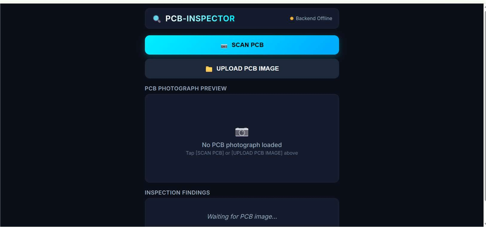
Instead of a separate Android app, the interface is a lightweight mobile web page (HTML + CSS + JavaScript) that opens in the phone browser. This works on any phone, needs no installation and can directly use the phone camera. The design is a dark theme with large touch-friendly buttons.
Interface flow
1. Open the PCB-INSPECTOR page on the phone; the status badge at top right shows whether the backend is online.
2. Press SCAN PCB → the camera opens → capture the PCB photograph (or press UPLOAD PCB IMAGE to choose an existing photo).
3. The photograph appears in the PCB PHOTOGRAPH PREVIEW panel.
4. Press Analyze → the image is sent to POST /api/inspect.
5. INSPECTION FINDINGS panel shows PCB PASSED / PCB FAILED with the lists of missing, misplaced and unexpected components.
Example result screen
+-----------------------------+
|         PCB RESULT          |
|         PCB FAILED          |
| Missing Components:         |
|   - C17                     |
| Misplaced:   - None         |
| Unexpected:  - None         |
+-----------------------------+
Connection Explanation
The system needs very little wiring because the “sensor” is the camera and the “processor” is the UNO Q. The connections and data paths are:
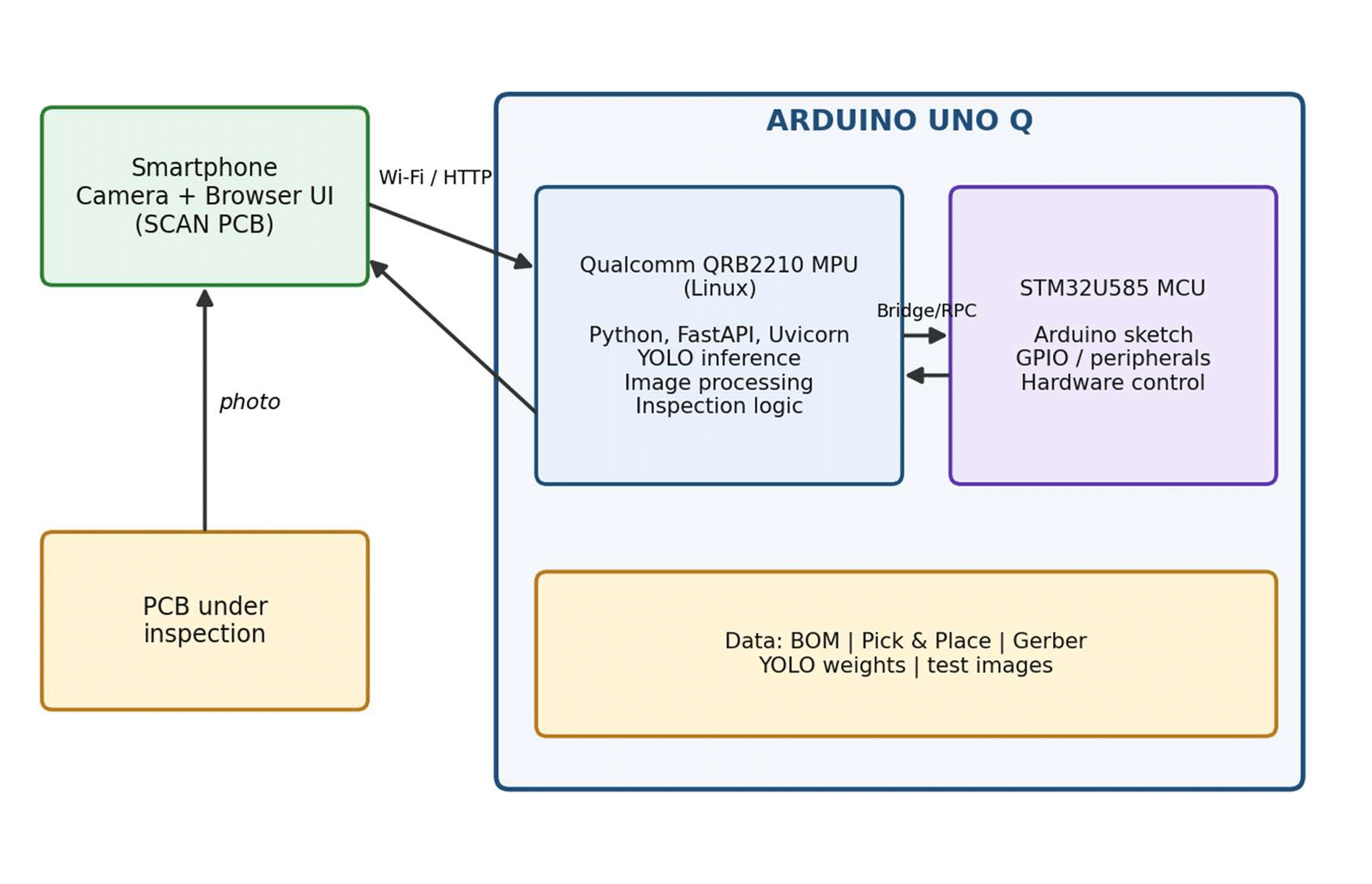
- Arduino UNO Q ↔ Computer: USB-C cable – powers the board and is used for programming/App Lab. The green and red LEDs in Fig 3 show the board is powered and running.
- Smartphone ↔ UNO Q / backend: Wi-Fi network using HTTP/REST; the phone sends the PCB image and receives the JSON result.
- Inside the UNO Q: QRB2210 (Linux) ↔ STM32U585 through Bridge/RPC.
- PCB under test: no electrical connection – it is only photographed; this makes the inspection completely non-contact and safe.
Development architecture vs final architecture
| Stage | Data path |
|---|---|
| During development | Phone → Wi-Fi → PC backend → AI + PCB inspection → result → Phone |
| Final target | Phone → Wi-Fi → Arduino UNO Q (AI model + image processing + BOM/P&P comparison) → inspection result → Phone |
Testing
Backend API test
The FastAPI service was started with Uvicorn and tested from the built-in Swagger page (Fig 6). GET /api/health returns the “ok” status for the PCB-INSPECTOR service and GET /api/model returns the AI model information and status, confirming the backend, routing and JSON responses work.
AI detection test
The trained YOLO model was run on camera footage of a development board that contains ICs, headers and connectors. In the demo video (Fig 1, Fig 9) the model draws boxes and labels on the components in real time:
| Class detected | Confidence scores observed | Comment |
|---|---|---|
| IC | 0.96, 0.92 | Large ICs on the board detected with high confidence |
| Header | 0.81, 0.65, 0.47, 0.29 | Pin headers detected; lower scores at odd angles / motion blur |
| Connector | 0.91, 0.53, 0.51, 0.26 | Connectors detected; confidence drops when the board is moving or partly out of frame |
Interface test
The mobile page loads with SCAN PCB and UPLOAD PCB IMAGE options, the preview panel and the findings panel (Fig 7). The status badge at the top confirms whether the backend is reachable.
Observations
- Detection works best with good lighting, a steady camera and the board filling the frame – this is why a fixed camera mount is planned.
- Confidence is lower on blurred or partial views; the inspection engine will use a confidence threshold to ignore weak detections.
- Because the AI only detects component types (not designators), the design is easy to extend to new boards by just loading a new BOM/P&P/Gerber set.
Project Development Status
| Phase | Work | Includes | Status |
|---|---|---|---|
| 1 | Hardware setup | UNO Q, App Lab, Python, Arduino, Bridge, STM32 | Completed |
| 2 | Backend | Health, Model and Inspection API (FastAPI) | Basic backend completed |
| 3 | Mobile interface | Home screen, SCAN PCB, camera, preview, analyse, result | Interface built; wiring to backend in progress |
| 4 | AI model | Dataset, training, validation, testing, inference | Proof-of-concept training completed; final checkpoint being re-trained/recovered |
| 5 | PCB data | BOM, P&P and Gerber parsers, expected PCB map | Planned |
| 6 | Inspection engine | Coordinate matching, missing / misplaced / unexpected, PASS/FAIL | Planned (logic designed – Section 6.5) |
| 7 | Edge AI | Model optimisation, export, UNO Q deployment, local inference | Planned |
| 8 | Final integration | Phone → camera → UNO Q (AI + PCB data + inspection) → result → phone | Planned |
Skills and Learning Outcomes
| Area | What is learned / applied |
|---|---|
| Electronics | PCB, components, BOM, Gerber, Pick & Place, PCB assembly defects |
| Programming | Python, C/C++, Arduino, HTML, CSS, JavaScript |
| AI / Machine learning | Dataset preparation, YOLO, object detection, training, validation, testing, precision, recall, mAP, model weights, optimisation |
| Computer vision | Image processing, bounding boxes, coordinates, confidence scores |
| Embedded systems | Arduino UNO Q, Qualcomm QRB2210, STM32U585, Linux, GPIO, Bridge/RPC |
| Networking & backend | Wi-Fi, HTTP, REST API, JSON, FastAPI, Uvicorn, file upload, model serving |
| Frontend | Mobile UI, camera access, image upload, API communication |
| System integration | Hardware + software, AI + PCB data, camera + AI, UNO Q + mobile, real-time inspection |
Applications, Benefits and Future Scope
Applications
- Quality check in small-scale PCB manufacturing and assembly lines.
- Student labs and hobby workshops verifying hand-assembled boards.
- Repair and service centres comparing a board with its reference design.
- Incoming inspection of PCBAs from contract manufacturers.
Benefits
- Low cost compared with commercial AOI machines.
- Portable, non-contact and quick – result within seconds.
- Consistent and objective; not dependent on operator fatigue.
- Reports exact designators (e.g., C17) so rework is fast.
- Edge processing: works offline and keeps design data private.
Future scope
- Fixed camera rig with controlled lighting and automatic capture.
- Automatic board alignment/registration using Gerber outline and fiducials.
- Additional defect types: wrong value/polarity, solder bridges, tombstoning.
- STM32 outputs: pass/fail LEDs, buzzer, reject actuator and conveyor control.
- Batch reporting and traceability (PDF/CSV reports, database of inspected boards).
- Quantised/optimised models for faster inference on the UNO Q.
Conclusion
PCB-INSPECTOR demonstrates a practical AIoT solution for automatic PCB inspection. By combining design data (BOM, Pick & Place, Gerber) with YOLO-based component detection and a comparison engine, it can report missing, misplaced and unexpected components and give a clear PASS/FAIL result. The Arduino UNO Q provides both the Linux/AI processing and the microcontroller-based hardware control in a single low-cost board. The hardware setup, FastAPI backend, mobile interface and proof-of-concept AI detection are already working, and the remaining phases – PCB-data parsing, the inspection engine and on-device deployment – are clearly defined. The project is being developed and submitted by Saran Ramalingam (individual participant), SREC, Coimbatore, for the AIoT Design Challenge 2026.
References:
- wangshnegqi, “pcb-component-detection-dataset-yolo”, GitHub repository (dataset, labels, data.yaml and YOLOv8 PCB weights).
- Ultralytics YOLOv8 documentation; FastAPI documentation; Arduino UNO Q / Arduino App Lab documentation.
