



From PCB To Optical: Selecting The Right High-Speed Interconnect Architecture For AI And Data Centre Systems
Not only processor speed is being improved by training clusters for AI, hyperscale cloud and high-performance computing. The data flow architecture is being altered too. Contemporary servers contain multiple GPUs, CPUs, accelerators, fast memory, storage and network components providing communication channels that could be formed of several boards and various mediums. The next-generation interconnects such as PCIe Gen5 & Gen6, high-speed Ethernet, accelerators fabric and new generation rack-scale platforms are capable of delivering an increased amount of data through the channels.
With growing signaling speed, the interconnect cannot be considered anymore as a mere mechanical coupling of two components. PCB traces, connectors, cables, optical links and backplanes all affect the channel budget. In reality, the communication channel performance may define whether the system reaches its desired throughput, density, thermal and maintenance capabilities.
This leads to a change in engineering paradigm, where instead of determining what connector can support a certain data rate, engineers are forced to think about what set of interconnect technologies will create the optimal end-to-end channel.
Why High-Speed Interconnect Selection Matters More Than Ever
Now think about an AI training server in which multiple GPUs communicate with each other along with CPUs, memory components, and fast network interfaces. The same applies to inference servers, storage systems, and Ethernet switches, where ever-increasing amounts of data need to be transferred between computing and networking components.
Increasing speed of signaling makes the physical medium more unforgiving. Insertion loss lowers the signal strength as it propagates on the copper medium; return loss is caused by impedance mismatches; and crosstalk couples unintended signals between neighboring channels. Discontinuities are caused by vias, connectors, and transitions, while longer PCB paths make the medium more vulnerable to dielectric and conductor losses.
All of these factors reduce the available margins for timing and voltage at the receiver side. The designer might use transmitter and receiver equalization as compensation, although equalization itself may increase complexity and power dissipation. On the other hand, dense routing increases the difficulty of the PCB layout, whereas powerful processors and accelerators create their own requirements for the thermal design and airflow considerations.
Moreover, EMI becomes increasingly critical. An accelerator board packed with components will include hundreds of fast differential pairs along with power conversion circuitry, clocks, and many other signals. Controlled impedance, proper spacing, and correct grounding and return paths become a necessity.
In turn, interconnect becomes part of the system architecture rather than a packaging concern. The interconnect plays an important role in the scalability of the bandwidth, number of layers on the PCB, mechanical design, thermal behavior, manufacturing complexity, and upgradability of the platform.
Why PCB Routing Alone Is No Longer Enough
PCB traces are very much essential for high-speed systems, but they do not necessarily have to be the optimal solution for all portions of the signal path. In the case of a shorter and well-designed PCB trace, an efficient electrical connection can be achieved. But it is the difficulty with a longer trace involving many vias, connectors, and highly dense portions of the PCB that creates the problem.
“Encryption on the hardware is the first layer of security. Any data which goes outside the hardware needs to be encrypted on the hardware and then taken out” said Jash Jetly, co-founder and CEO of EVE NET
As the data rate increases, it becomes important to take into account dielectric loss, conductor loss, impedance mismatch, via reflections, skew, crosstalk, and EMI. Extending a high-speed electrical connection would mean adding more PCB layers, stack-up considerations, and tighter tolerance levels. This does not mean that PCB traces are no longer relevant in such situations. What it means is that new designs now involve a combination of PCB traces with connectors, cables, optics, and backplanes.
Understanding The Complete Signal Path
A modern computing platform does not normally employ a single interconnect technology from beginning to end. For instance, a system’s accelerator card could employ PCB traces to link its processor to a connector. Board-to-board links could be employed to connect this accelerator card to another PCB, while a high-speed cable could help reduce losses in a particular area of congestion on the board. Optical connectivity, on the other hand, could be used to transport the data off the PCB for longer electrical routes. Finally, backplane technology could enable communication between multiple boards at the chassis level.
It is therefore the task of an engineer to optimise the entire channel, and not simply to maximise the performance of a single link. Now imagine a GPU cluster having several accelerator cards installed. The high-frequency signals may be routed via the PCB paths on each accelerator card, via a high-density board-to-board connector to connect with the system board and then via a cable to skip certain parts of lossy PCB. If the distance between processing and networking becomes too big, the optical flyover is a means to route the data without keeping the whole path electrically connected.
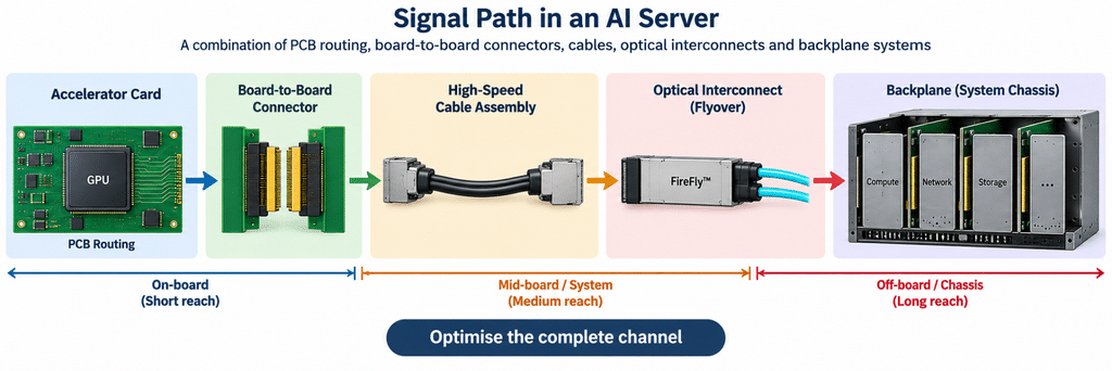
At the chassis level, a backplane can then connect compute, networking, or storage modules. In this architecture, copper and optical technologies are complementary. Copper remains attractive for compact, short-distance connections, while cables and optical links can be introduced selectively where PCB routing or electrical transmission becomes more difficult.
High-Density Board-to-Board Connectivity For Compact Computing Platforms
The increasing amount of processing capability being packed into accelerator cards, server blades, and networking equipment makes board-to-board density increasingly important. A connector must provide more than a large number of contacts. Its pitch, stack height, contact design, grounding arrangement, and routing flexibility all affect the usable PCB area and signal-integrity performance. Mechanical robustness also matters in systems where boards may need to be installed, removed, or replaced during maintenance.
The SEAM terminal from SEARAY™ (SEAM/SEAF Series) architecture illustrates this approach through an open-pin-field arrangement that allows engineers to configure signal, power, and ground assignments according to the requirements of the board. It also covers single-ended or differential pair configurations. It supports up to 56Gbps PAM4 performance and can provide up to 560 single-ended I/Os or 140 differential pairs, depending on the configuration, with stack heights ranging from 7mm to 18.5mm.
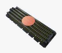
The open-pin-field concept is particularly useful when the PCB layout needs flexibility. For example, an FPGA module can use a dense board-to-board connection to communicate with a carrier board without requiring a large connector footprint. Similarly, an AI accelerator or networking line card can use the available contact field to organise differential pairs, grounds, and other signals around the physical constraints of the PCB. The benefit is not simply connector density. The architecture allows the mechanical interface and the PCB routing strategy to be considered together.
High-Speed Cable Assemblies: Extending Performance Beyond PCB Routing
As board layouts become more crowded, routing a high-speed connection entirely through copper layers can create a difficult trade-off between signal integrity, board area, and mechanical freedom.
A cable can provide another option. Instead of forcing a differential pair through a long PCB route, the connection can be taken above the board and routed around processors, memory devices, power circuitry, or other obstacles.
The 612-ARC6-08-12.0-LU-LD-2-1-ND from ARC6/ARF6 family provides an example of this approach. Its direct-attach architecture connects the cable directly to the contacts, avoiding the transition board normally used between a cable and connector. The assembly supports 64 Gbps PAM4 (32 Gbps NRZ), PCIe 6.0 / CXL 3.2 capable. Its slim two-row construction is designed for high-density applications.
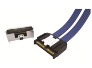
This type of architecture can be useful in an accelerator server where a processor and expansion card are physically separated by a region occupied by power circuitry. Rather than adding PCB layers and routing channels through the congested area, the designer can take the signal off the board and route it over the obstruction.
The result can be greater layout flexibility while also supporting serviceability. A replaceable cable assembly can provide a more practical modular approach than redesigning a multilayer PCB simply to accommodate a longer electrical route. The same principle applies to storage platforms and networking equipment, where the optimum physical route may not follow the shortest distance across the PCB.
When Optical Interconnects Become The Better Choice
Electrical interconnects remain highly effective over short distances, but attenuation and insertion loss become increasingly challenging as transmission distances and aggregate bandwidth increase.
This is one reason optical connectivity is becoming part of the interconnect strategy in large AI and networking systems. Optical transmission is largely immune to electromagnetic interference along the optical path and can carry high-bandwidth signals over distances that may be difficult to support with conventional PCB traces or copper cables. The objective is not to replace every electrical connection with optics, but to introduce optical links where they provide a system-level advantage.
The FireFly™ ETUO is an example of an active optical micro-flyover approach in which the data connection is taken off the PCB. It supports performance up to 25.7 Gbps for ETUO and 112 Gbps PAM4 for the FireFly optical roadmap. It incorporates an integral heat sink for thermal management. Its extended temperature has a -40 ºC to +85 ºC range for military and industrial applications (ETUO).
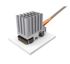
Imagine a high-performance switch with processing devices concentrated near the centre of a PCB while optical or network interfaces are positioned elsewhere on the board. Routing every high-speed electrical connection through the board can consume valuable routing space and increase loss. An optical flyover can instead take selected channels above the PCB, allowing the electrical portion of the path to remain shorter.
Backplane Connectivity For Modular AI And Networking Systems
Large systems introduce another challenge: multiple boards must communicate through a common chassis while remaining modular enough for installation, maintenance, and future expansion.
Backplanes address this requirement by providing a common interconnect infrastructure for compute, networking, or storage cards. They are widely used in modular network switches, telecom equipment, and storage systems, and they remain relevant as AI infrastructure becomes increasingly modular.
The ExaMAX® system demonstrates how a high-speed backplane architecture can combine density with signal-integrity and routing considerations. The system supports board-to-board configurations up to 64 Gbps PAM4 (32 Gbps NRZ) on a 2.00 mm column pitch, while Flyover cable configurations support data rates up to 112 Gbps PAM4. Its signal wafers incorporate a one-piece, embossed ground structure that improves isolation and reduces crosstalk.
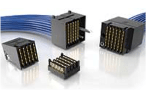
For a modular Ethernet switch, for example, line cards can communicate with a central switching or processing board through the backplane. A similar architecture can allow storage modules to connect to shared processing resources without requiring each module to have an independent point-to-point cable infrastructure.
Selecting The Right Interconnect Architecture: There Is No One-Size-Fits-All Solution
The four architectures described above should not be viewed as competing technologies. Each solves a different part of the system-level interconnect problem. A short connection between devices on the same PCB may be best handled with conventional controlled-impedance routing. A dense connection between two closely spaced boards may favour a high-density board-to-board connector. A longer connection across a congested board may benefit from a cable assembly. A still longer or particularly loss-sensitive path may justify optical connectivity. A chassis containing many modular boards may require a backplane architecture.
The selection process should therefore begin with the complete channel.
| Architecture | Best suited to | Main advantage | Key design consideration |
| PCB routing | Short, controlled board-level paths | Compact and integrated | Loss, vias, impedance, and routing complexity |
| Board-to-board | Dense modular PCB connections | High density and space efficiency | Pin assignment, stack height, and signal integrity |
| Cable assembly | Longer or obstructed board-level paths | Routing flexibility and serviceability | Cable loss, skew, mechanical routing |
| Optical interconnect | Longer, high-bandwidth paths | Low-loss transmission and EMI immunity | Optical transceivers, thermal management, and system placement |
| Backplane | Multi-board chassis architectures | Modular connectivity and scalability | Density, crosstalk, mechanical alignment, and channel budget |
The decision should be based on bandwidth, physical distance, channel loss, latency, routing difficulty, connector density, thermal constraints, and expected future upgrades—not simply the headline data rate of a connector.
Real-World Applications Across AI And Data Centre Infrastructure
In an AI training machine, board-to-board connectivity can provide dense communication between accelerator modules and a system board, while cable assemblies can route signals around mechanically or electrically congested areas.
A GPU cluster introduces another level of complexity. Accelerator cards may communicate electrically within a server, while optical links can become attractive for longer connections between equipment where copper would introduce excessive attenuation or equalisation requirements.
Network switches provide another clear example. Short PCB paths can connect switching devices to local interfaces, while high-density connectors provide board-to-board communication. A backplane can then form the common infrastructure between multiple line cards.
Telecommunication equipment places additional emphasis on mechanical robustness and serviceability because individual modules may need to be replaced without redesigning the entire system.
At the hyperscale level, the architecture becomes even more heterogeneous. Thousands of servers, switches, storage systems, and accelerators may coexist within a facility, making the physical interconnect strategy an important contributor to power, cooling, density, and maintenance requirements.
Future Trends In High-Speed Interconnect Design
The trajectory toward higher signaling rates is unlikely to reduce the importance of interconnect engineering. It will make it more important. Technologies such as 224G PAM4, PCIe Gen6, and future PCIe generations, CXL, UCIe, co-packaged optics, and 800G/1.6T Ethernet are increasing the amount of information that must move through a constrained physical infrastructure.
At these speeds, even small discontinuities can consume a meaningful portion of the channel budget. Engineers will increasingly need to optimise connectors, packages, PCB transitions, cables, and optical interfaces together.
AI rack-scale architectures could further change the physical relationship between compute, memory, and networking resources. Instead of designing each server as an isolated unit, system architects are increasingly considering the rack as a larger computing platform. This trend strengthens the case for hybrid interconnect architectures. Copper will remain valuable for short, dense, and cost-sensitive connections. High-speed cable assemblies can extend electrical reach while bypassing difficult PCB regions. The future is therefore unlikely to be purely electrical or purely optical. It will be a carefully engineered combination of both.
| S.NO | Digikey Part Number | Specs | Brand | Direct Links |
| 1. | SEARAY™ (SEAM/SEAF Series) | 1.27 mm-pitch, high-density board-to-board terminal supporting 56 Gbps PAM4, up to 560 single-ended I/Os or 140 differential pairs, and 7mm–18.5mm stack heights. | Samtec | click here |
| 2. | ARC6/ARF6 | AcceleRate is a 0.635 mm pitch Eye Speed ultra-low skew twinax cable with direct attach to the contacts | Samtec | click here |
| 3. | FireFly™ ETUO | Embedded and rugged optical transceivers make data connections ‘off board’ for up to 25.7 Gbps per lane with a path to 112 Gbps PAM4 via optical cable at greater distances, or copper for cost optimisation. | Samtec | click here |
| 4. | ExaMAX® | High-density backplane systems offer design flexibility for various applications, including Flyover cable supporting 112Gbps PAM4 and board-to-board supporting 56Gbps PAM4. | Samtec | click here |
| Design Considerations Beyond Bandwidth |
| Data rate is only one parameter in the interconnect decision. Engineers should evaluate: • Insertion and return loss: How much of the signal budget is consumed by the complete channel? • Crosstalk: Are adjacent differential pairs sufficiently isolated? • Skew: Do signals within a differential pair or across lanes arrive within the required timing window? • Latency: Does the selected architecture introduce unacceptable propagation or conversion delays? • EMI: Could the physical routing create interference with nearby circuits? • PCB routability: Can the required channels be routed without excessive layers, vias, or congestion? • Thermal behaviour: Can connectors, active optical devices, and cable paths operate within the available thermal envelope? • Airflow: Will the physical interconnect arrangement obstruct cooling paths? • Mechanical robustness: Can the connection withstand mating, vibration, and servicing requirements? • Scalability: Can the architecture support the next generation of processors, accelerators, and networking speeds? This system-level approach is particularly important because improving one part of the channel can sometimes create a problem elsewhere. A shorter PCB route may require a more complex cable arrangement. A denser connector can save board space but introduce additional signal-integrity considerations. Optical connectivity can solve electrical loss problems while introducing optical-module and thermal-management requirements. The objective is not to select the most advanced technology available. It is to allocate each section of the signal path to the technology that handles its particular constraints most effectively. |
+++++ BOX ITEM +++++
| Quick Selection Guide: Choosing The Right High-Speed Interconnect Architecture |
A practical decision sequence for engineers can begin with five questions: 1. How far must the signal travel? For short paths, PCB routing may remain the simplest solution. As distance increases, evaluate cables or optical links. 2. Is PCB routing becoming a constraint? If long routes require additional layers, complex via structures, or difficult breakout regions, consider taking the signal off-board. 3. Is board density the primary problem? For compact accelerator, FPGA, or networking modules, a high-density board-to-board architecture can maximise usable PCB area. 4. Is electrical loss becoming difficult to manage? If attenuation and equalisation requirements consume too much of the channel budget, investigate optical connectivity for the affected section. 5. Does the system require modular boards? If multiple compute, storage, or networking cards must share a chassis, a backplane architecture can provide the necessary scalable infrastructure. |
Common Design Mistakes
- Using PCB traces simply because they are available: A theoretically routable connection may consume excessive layers or create an impractical loss budget.
- Selecting purely on headline data rate: A connector rated for a target signaling rate does not guarantee that the complete channel will meet system requirements.
- Ignoring insertion loss: Connectors, vias, transitions, and PCB materials all contribute to the total channel loss.
- Treating thermal management as a separate problem: Cable paths, active optical devices, and dense connector regions can influence airflow and heat dissipation.
- Optimising one connection instead of the complete channel: The transmitter-to-receiver path should be evaluated as a complete system.
- Designing without future scalability: A connection that works for today’s signaling rate may become a bottleneck as processors, accelerators, and networking interfaces move to higher bandwidth.
The most important change in high-speed interconnect design is not the emergence of one particular connector or cable technology. It is the recognition that the communication channel itself has become a system-level design element. A modern AI or data-centre platform can contain PCB routing, board-to-board connections, high-speed copper cables, optical flyovers, and backplane systems within the same signal architecture. Each technology has a role.
The engineering challenge is to determine where that role begins and ends. For a compact accelerator board, density, and routing flexibility may dominate. For a connection crossing a congested PCB, cable-based routing may provide a better balance. For a longer high-bandwidth path, optical transmission can avoid some of the limitations associated with long electrical channels. For a modular chassis, the backplane remains a practical foundation for connecting multiple boards. As AI workloads continue to drive bandwidth, density, and scalability requirements, successful designs will increasingly come from optimising these technologies together rather than selecting one technology in isolation. The future high-speed platform will therefore not be defined by PCB, copper, or optical connectivity alone. It will be defined by how intelligently engineers combine them to deliver the required signal integrity, bandwidth, thermal performance, manufacturability, serviceability, and upgrade path across the complete system.

