




A proposed tiny tape-out programme could funnel college chip-design projects into a pipeline with Indian fabs, giving students practical experience to take designs towards fabrication.
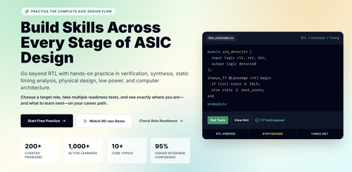
An Indian edtech startup, SiliconSprint, which offers an online platform like LeetCode for very large-scale integration (VLSI) and chip-design engineers to practise Verilog and SystemVerilog, aims to build a tiny tape-out programme for India. “There is a significant push towards VLSI and semiconductor manufacturing in the country, but developing fabrication facilities alone is not enough. We also need a talent pool that understands how to design chips,” said an authorised spokesperson from SiliconSprint in a recent interaction with Electronics For You (EFY).

The company wants to create a system where students from engineering colleges can get real‑world experience in chip design. Students will create graphic design system (GDS) files. Ultimately, they will have their designs actualised. This will help build a flow of chip designs for fabrication facilities. To achieve this, the startup is trying to collaborate with universities so that they can introduce chip‑design capstone projects as part of their curriculum. The professors will teach the theory while students will use the platform to practice.
For instance, when the platform interacts with 10 universities, with 100 students in each university, the platform may help come up with 1000 designs in each semester. Such student designs may form the customer base for fabrication facilities using the 180nm technology. With the shuttle program running in the fabrication facilities, such student designs can become part of the fabrication runs, whereby students will be able to have hands-on training on the whole process of manufacturing chips, and the fabrication facilities will have designs that will enable them to fill up their shuttle programs. This is an innovative vision of the startup.
The objective here is to guide the students from the process of register-transfer level (RTL) design to the GDS files that can be fabricated. The startup is contemplating a concept where students do these projects in each semester.
It is easy to notice the tape-out projects in those countries wherein more advanced students studying VLSI are able to design a tiny chip and submit it for fabrication in a common production batch. Let us assume that the price for one common chip fabrication batch equals US$20,000; the cost could be split among 200 participants, with each contributing around US$100–200. Each student would be assigned part of a common chip design which needs to be submitted for fabrication. The company is planning to implement a similar project in India in order to provide students with practical experience.
The startup has initiated contact with the institutes, including IITs and NITs, for collaboration. Several professors from the NITs have shown interest and suggested implementing the SCL 180nm process design kit (PDK) into SiliconSprint’s platform. The company is looking into these suggestions; however, the talks are still at the preliminary stages, and no formal university partnerships exist yet.