
A buck converter is a DC-DC power converter that efficiently steps down a voltage. It uses an inductor, resistors, and a capacitor to regulate the output, making it particularly suitable for wearable electronics and IoT devices.
The following Open Source license covers this project: Creative Commons Non-Commercial Similar Adaptations. For commercialisation of our designs, please email to [email protected]. For full details of this license, please refer to the license details published at the end of this project.
Table of Contents
POC Video Tutorial
Low-dropout regulators (LDOs) offer a more straightforward approach to voltage regulation, but they often dissipate significant heat, thereby reducing efficiency in compact, power-sensitive systems. Buck converters offer a more efficient solution, but adding an inductor increases the design footprint.
This compact converter design is based on a buck converter IC. The complete power system, including the converter, fits within a 9mm footprint—ideal for space-constrained applications while leaving room for other essential components.
A key feature is its ability to deliver variable output voltages from 1.2V to 3.3V DC by replacing a fixed resistor with a potentiometer. This enables fine-tuned voltage adjustment to match the specific needs of each device.
The converter may be used as a standalone variable-voltage module or integrated directly into wearable electronics.
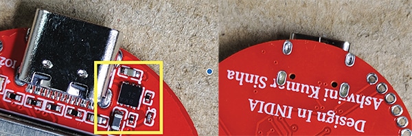
The converter is embedded in the device’s PCB, delivering the required output voltage range with over 93% efficiency and no thermal issues. The design incorporates the PAM2305D SMD IC, housed in a compact DFN-6 (2×2mm) package. Fig. 1 shows the author’s DC-DC buck converter integrated into the custom-designed PCB.
According to the datasheet for the IC selected for this converter design (see the datasheet for details), the design requires an inductor, several resistors, and capacitors. If a variable output voltage is desired, a potentiometer can be used. The complete list of needed SMD components is provided in Table 1.
| Table 1: Bill of Materials | |||||||
| Name | Designator | Footprint | Quantity | Manufacturer Part | Manufacturer | Supplier | Supplier Part |
| 10µF Capacitor | C1, C2 | C0402 | 2 | CL05A106MP5NUNC | SAMSUNG | LCSC | C315248 |
| 100pF Capacitor | C3 | C0201 | 1 | GRM0335C1E101JA01D | muRata | LCSC | C76917 |
| 4.7µH Inductor | L1 | L0603 | 1 | CMH160808B4R7MT | FH | LCSC | C394952 |
| 500kΩ Resistor | R1 | RES-ADJ-SMD_3P-L3.8-W3.7_VGF39NCHXT | 1 | VGF39NCHXT-B504 | HDK | LCSC | C22461638 |
| 120kΩ Resistor | R2 | R0201 | 1 | 0201WMF1203TEE | UNI-ROYAL | LCSC | C270362 |
| USB 2.0 Solder Pad | U1 | USB SOLDER PADS | 1 | USB-TYPE-C-018 | DEALON | LCSC | C2927038 |
| PAM2305DGFADJ | U8 | DFN-6_L2.0-W2.0-P0.65-BL-EP | 1 | PAM2305DGFADJ | DIODES | LCSC | C780869 |
| Potmeter SMD (Fig. 5) | R1 (Fig 5) | RES-ADJ-SMD_3P-L3.8-W3.7_VGF39NCHXT | 1 | VGF39NCHXT-B504 | HDK | LCSC | C22461638 |
Buck Converter Circuit Design
The buck converter IC (PAM2305DGFADJ) comes with six pins. According to the datasheet, the application circuit includes a VIN pin for the input voltage, a GND pin for grounding, and an FB pin that receives feedback to regulate the output voltage. The EN (Enable) pin controls the IC’s operation when tied to a pull-up resistor or directly to the input voltage, enabling the IC to be active. When pulled low, the converter is disabled. The SW (Switch) pin connects to an inductor, and the output voltage is set by two resistors connected between SW, FB, and GND. Fig. 2 shows the IC (PAM2305DGFADJ) datasheet pinout and application circuit.