

The open-source YuzukiNeko development board combines a RISC-V multimedia SoC, 16 MiB PSRAM and 16 MiB NOR Flash in a Raspberry Pi Pico-style form factor.
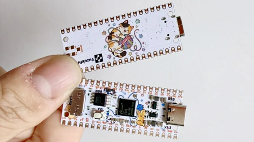
YuzukiHD has released YuzukiNeko, a compact open-source development board built around the Allwinner F101S3, also identified in its documentation as the SUN252I-F101. Rather than positioning the board as a conventional microcontroller platform, YuzukiNeko brings a XuanTie C907 RISC-V processor and multimedia capabilities into a Raspberry Pi Pico-style hardware layout, targeting graphics, display, audio and general-purpose embedded projects. The hardware design is released under the CC0 1.0 Universal licence.
The board uses the F101S3 SoC in a 7 mm × 7 mm QFN68 package, featuring a 32 KB instruction cache and 16 KB data cache. It integrates 16 MiB of SiP PSRAM and 16 MiB of external NOR Flash with execute-in-place (XIP) support. A USB-C connector, microSD card socket and an FEL button are also included on the board. Its expansion interface follows the familiar 2 × 20-pin Raspberry Pi Pico-style header arrangement.
The F101S3 provides considerably broader peripheral support than a typical small microcontroller board. Available interfaces include USB 2.0 DRD, SDIO 2.0, two SPI controllers, six UART interfaces, three TWI interfaces, two CAN controllers, PWM, infrared reception, GPADC and TPADC. The CAN interfaces expose logic-level signals, meaning an external CAN transceiver and appropriate bus termination are required when connecting to a physical CAN network.
The multimedia hardware supports JPEG decoding up to 16,384 × 16,384 pixels, PNG decoding up to 2,048 × 2,048 pixels, and JPEG/MJPEG encoding up to 720p at 30 frames per second. Display capabilities include RGB888 output up to 1280 × 720 at 60 Hz, single-link LVDS up to 1366 × 768 at 60 Hz, and four-lane MIPI DSI up to 1280 × 800 at 60 Hz. Audio interfaces include a DAC, I2S/PCM and OWA output.
The project also provides hardware files and board support, while a separate Buildroot external tree includes configurations for building RAM-disk and NOR Flash firmware images for YuzukiNeko. The NOR image layout incorporates the bootloader, device tree, OpenSBI firmware, Linux kernel and root filesystem within the board’s 16 MiB Flash.
One hardware issue documented for the V1.3 PCB is an incorrect PD GPIO numbering sequence on the silkscreen, which was corrected in V1.4. Developers using V1.3 boards need to account for this numbering offset when configuring pin multiplexing.
For more information, click here.