





A new clock-buffer family helps bridge low-voltage processors and higher-voltage components while improving signal integrity and simplifying board design for advanced systems and high-speed applications.
with Higher Voltage Components
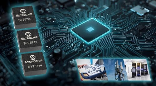
Microchip Technology has introduced the SY757xx family of 1.2V-output LVCMOS clock buffers, designed to simplify clock distribution between low-voltage processors and higher-voltage components in FPGAs, SoCs, AI accelerators and next-generation CPUs. The devices combine voltage translation with low additive jitter, helping designers maintain signal integrity while reducing board-level complexity.
As advanced semiconductor processes increasingly operate at lower supply voltages, conventional clock-buffer solutions can require discrete components and voltage-divider circuits. These approaches can introduce duty-cycle distortion, compromise signal quality and increase component count. The SY757xx family addresses this by integrating voltage translation into a single-chip solution.
The clock buffers support a broad supply-voltage range and can translate signals across a 1.2V to 3.3V input range. Microchip specifies additive jitter below 25 femtoseconds and operation across a frequency range extending up to 250MHz. This enables clock signals to be distributed between different voltage domains while maintaining timing accuracy.
The family is intended for applications where precise clock distribution and fanout are important, including high-speed parallel processing, hardware reconfigurable systems, low-latency computing, real-time processing, AI and machine-learning acceleration, industrial control, IoT, networking and communications equipment.
Microchip has developed the devices in several configurations and compact packaging options. The portfolio includes differential and single-ended input choices, different voltage-translation ranges and output-enabled fanout options. The devices are housed in space-saving eight-pin packages.
By replacing discrete voltage-divider and buffer arrangements, the SY757xx family can reduce component count and simplify PCB design. It can also help improve AC coupling and biasing while maintaining clock integrity across different voltage domains.
The new buffers are aimed at designers developing increasingly dense computing and embedded systems. Their combination of low-voltage operation, voltage translation and low jitter provides a practical approach to clock distribution in systems where timing accuracy and board space are increasingly important.
