


Can panel-level packaging scale without compromising yield? New dispensing and plasma systems address warpage, surface preparation, and process consistency.
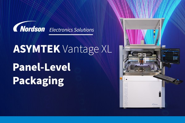
Nordson Electronics Solutions has showcased two systems for panel-level packaging (PLP), targeting process challenges that arise as semiconductor manufacturers move towards larger panels for higher throughput and lower-cost advanced packaging at the Semicon 2026.

PLP can process more packages in a single manufacturing cycle than conventional wafer-based approaches, making it relevant to growing demand for AI and high-performance computing. However, larger panels can introduce challenges such as warpage, thermal effects, surface uniformity, and dispensing accuracy that can affect packaging yield.
The ASYMTEK Vantage XL addresses the dispensing stage by applying underfill to larger panel formats. The system is designed to improve underfill flow while helping manage panel warpage, supporting more consistent and void-free results. These capabilities are intended to help manufacturers develop and scale advanced packaging processes while maintaining dispensing accuracy and throughput.
Surface preparation is handled by the MARCH ExoSPHERE plasma treatment system, which is designed for both panel- and wafer-based packaging processes. Plasma treatment activates and cleans surfaces before subsequent processes, helping improve adhesion and process consistency for applications including underfill.

The ExoSPHERE uses a three-axis symmetrical chamber to provide uniform plasma treatment across panels measuring up to 650 × 650 mm. Integrated handling accommodates both panels and wafers and can adapt to panel warpage, while process controls are designed to maintain repeatable treatment from one panel to another.
Together, the systems address two different stages of advanced packaging: preparing surfaces for reliable bonding and accurately dispensing materials across larger substrates. This becomes increasingly important as manufacturers explore larger panel formats to improve production efficiency without allowing substrate-related variations to undermine yield.
Click here for the official announcement.