




A software system combines chip and substrate images to support die placement without using a physical optical beamsplitter.
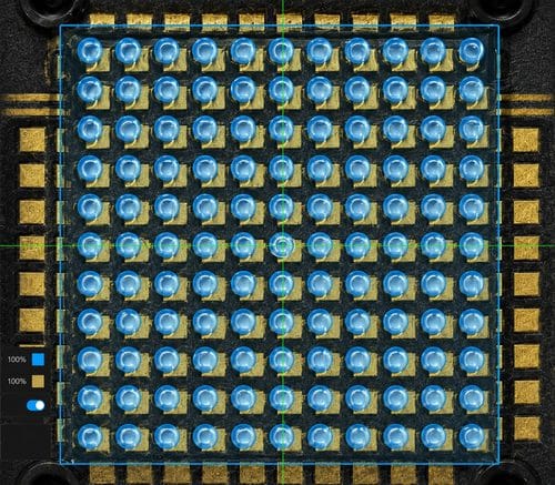
Tresky GmbH has developed a digital approach to visual alignment for high-precision die bonding that replaces the conventional optical beamsplitter with software-based image processing.
The system uses two cameras to capture different views during alignment. An upward-facing camera captures the chip, while a downward-facing camera captures the substrate or target position. Software combines the two images and displays them as a single alignment view.
In conventional systems, a physical beamsplitter combines light from the two optical paths. The additional glass sits directly in the beam path and can introduce reflections, ghost images and focus shifts. It can also reduce the light reaching the cameras and requires precise mechanical and optical alignment.
Tresky moves the image-combination function from the optical system to software, reducing the number of optical and mechanical variables in the alignment system.
The combined image allows the operator to see the chip structure, target structure and their relative misalignment in one view. Alignment can be performed along the X, Y and theta axes using direct visual feedback.
The software also allows parameters such as transparency, scaling, zoom, contrast, brightness and rotation to be adjusted for different applications. Additional overlays can be added to the alignment view.
The approach can address situations where a relevant chip structure or alignment mark becomes hidden after the chip has been picked up. A conventional optical system cannot display a feature that is physically blocked by the pickup tool.
Tresky’s system can capture the relevant chip structure before pickup and store it as a reference image. After pickup, this stored image can be overlaid on the live image of the substrate. The previously captured structure can therefore remain available as an alignment reference even when it is no longer physically visible.
The digital approach is intended for die bonding applications in research and development, prototyping, high-mix and low-volume manufacturing, photonics, optoelectronics and advanced packaging. It is particularly applicable where component geometries change frequently, or alignment depends on structures that may become obscured during the bonding process.


