


DesignSpark PCB is a schematic and layout design software. In this article, we explore the capabilities of this software, highlight the new features that came in its latest version, and also shed light on DesignSpark Mechanical.
DesignSpark PCB is a powerful, professional and completely free schematic and layout design software. Ideal for use in professional design environment, it currently claims over 250,000 users worldwide. DesignSpark PCB is easy to learn and comes with an intuitive user interface. It features context-sensitive toolbars, context-sensitive help, customizable shortcuts, interaction bar, easy access to all relevant commands and an online library of components—ModelSource—with some reference designs.

DesignSpark PCB also has online video and text tutorials to help users get started and a dedicated technical forum for technical clarifications. It improves itself based on community feedback, and further software development, enhancements and new features are derived from comments, design work and experiences shared by other members at DesignSpark’s forum.
DesignSpark PCB is offered completely free of charge and fully featured. (There are no intentional restrictions on designs) There are unlimited schematic sheets per project, up to one metre square of board size and no limits on layers—all of which allow you to get your creativity flowing without restraint. DesignSpark PCB circuit design software can be used for schematic capture, PCB board design and layout, generating impressive 3D view to visualise your design in real time and generate manufacturing files.
Compatibility
DesignSpark PCB supports importing of CadSoft Eagle PCB CAD design files, circuit diagrams and libraries. In addition to extensive libraries, sophisticated part-creation wizards make it easy to design new parts from scratch or by amending downloaded symbols and footprints. Bill of materials (BOM) report can also be generated at any time.

DesignSpark PCB allows you to generate all the files required to take your project from circuit diagram to layout schematic to a circuit-board built project. Gerbers (extended RS-274-X), excellons and component position reports are available to make your design compatible with pick-and-place machines ready for automated PCB assembly (reflow oven process). Other output formats include DXF (import and export) and IDF for interfacing to mechanical CAD software tools.
Key Features
Let us take a look at some of the key features of this tool:
Reference Designs:
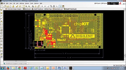
DesignSpark PCB has reference designs for hardware evaluation modules and development kits with complete schematics, PCB files and detailed documentations. Designers can save a lot of their time by using these designs and modifying them according to their requirements. The reference designs include, for instance, a chipKIT Max32 kit based on Microchip processor and motor control using Fairchild FNB41060.
ModelSource:
ModelSource is an online library of PCB and schematic components with over 80,000 of them. Designers can add components in their designs from ModelSource library and, while doing so, they can see various parameters of the components, manufacturers’ details, data sheets and components preview.
Simulation Interface:
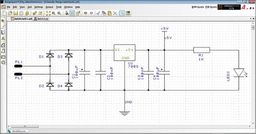
The Simulation interface consists of Simulation Output, SPICE libraries and Simulation Netlist. For Simulation Output, DesignSpark PCB has built-in SPICE parameters that can be assigned to components so that a number of circuit elements could be output to a number of standard SPICE simulators. SPICE simulators supported in DesignSpark PCB are LsSpice, LTspice, B2spice and TINA.
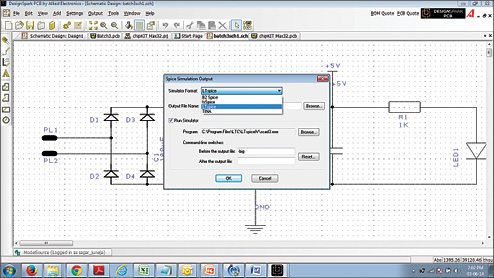
SPICE libraries available contain commonly-used components and symbols, including circuit stimuli and probes to help designers quickly generate circuits to simulate. SPICE Netlists writes a description of the devices in the circuit using basic SPICE format.
The simulation interface lets designers analyze various simulation responses (like AC response, DC response, transient response) of their schematic in one of the above simulators. This saves a lot of time for designers as they need not make a schematic separately in the simulation tool.
Library Creation and Components Wizard:
DesignSpark PCB gives freedom to designers to create new schematic symbols, PCB footprints and join them to form components that can be added to the user-defined library. Also, since schematic symbols and PCB footprints are separate entities in DesignSpark PCB, by using Components Wizard designers can create new components by providing a few parameters to pre-defined schematic symbols and PCB footprint. Components Wizard also helps designers link multiple schematic symbols with different PCB footprints and save the combinations as new components.
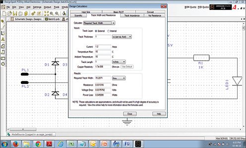
Design Calculators
Track Width calculator lets designers calculate the minimum track width based on the current it carries and temperature rise when current is applied. Track Impedance calculator calculates the characteristic impedance of a unit length of PCB track for a set of common track geometries. Via Resistance calculator calculates the resistance, voltage drop, power loss and thermal resistance of vias in a PCB design. Other design calculators available are for Heat Sink, RLCF and Conversion.
Design Rule Check
While designing a PCB, designers should keep in mind basic points like minimum track width, minimum annular ring, track-track clearance, track-pad clearance and pad-track clearance. Then there are other design rules related to nets, vias, drills and lot many things. When the Design Rule Check is run and errors found, textual error markers get added to the design with the appropriate code for that rule violation. This helps you identify and correct the error.
Auto-routing:
DesignSpark PCB supports complete auto-routing, partial auto-routing and manual routing. Using an auto-router to route even part of your PCB will give you a significant saving in time. And by combining the power of an auto-router with your experience in PCB layout, the resulting design can beat even the most labour-intensive manual layout results in terms of manufacturability, cost, and even aesthetics.
Forward Design Change and Back Annotations:
After translating schematic to PCB, if any changes are made in the schematic, the same can be transferred to PCB layout using Forward Design Changes option. It works to achieve netlist synchronisation between related schematic sheets and PCB designs. Design changes (addition/deletion) that are pushed forward include Net name, Connection/Net, Net class, Component, Component values, Component groups, Package, Pin changes.
Back Annotations let designers make changes in the PCB design and then apply those changes back to the master or original schematic design.
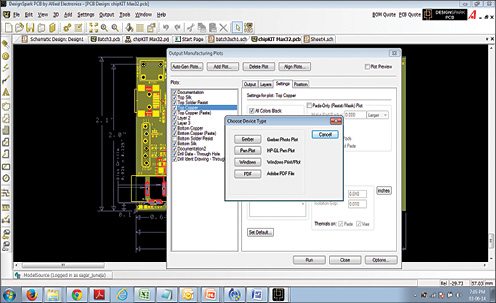
Manufacturing Plot (Auto-generating Plot)
Auto-generating plot lets designers automatically generate manufacturing plot. Auto-generation of plots for a design depends on the type of design and the type of output device selected. Designers may choose one of the following device types: Gerber, Pen Plot, Windows, PDF. Once the device type is chosen, designers may select what their set of plots should cover.
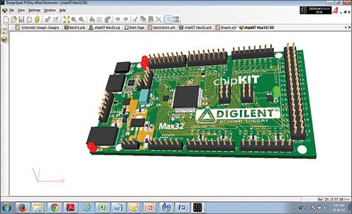
3D Viewer, DXF and IDF export. DesignSpark PCB supports 3D view of the PCB, which lets designers actually analyse how their PCB would look like physically. It uses a simple set of rules describing how each PCB symbol should be represented, together with various settings, like the thickness of the board, and uses the industry-standard OpenGL graphics toolkit to draw the 3D view.
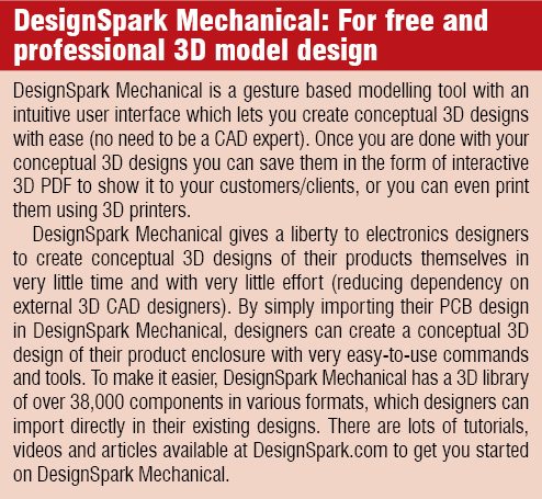
In addition, designers can export their PCB in MCAD tool for designing product enclosure. DesignSpark PCB supports two MCAD export formats: DFX and IDF. DFX output generates an AutoCAD DXF format file containing the board outline shape and the requested drill holes. The IDF format is used as an alternative to DFX by some MCAD (mechanical CAD) vendors for importing into their own systems. IDF files are exported in IDF 3.0 format. The IDF format is used by DesignSpark Mechanical (free and professional 3D model design software sponsored by RS Components) for importing board and component data from PCB design.
Good tool with a Good Ecosystem
 DesignSpark PCB has lots of technical resources available online to help designers easily learn and use the software. DesignSpark.com features video and text tutorials for designers to get started on DesignSpark PCB. There are also technical documentation on install and upgrade instructions, list of input/output file formats and lots of other information. A technical forum is also available on DesignSpark.com for specific technical clarifications and questions. Periodic releases of new versions of the software maximise designers’ experience as new versions are released based on users’ feedback and are available for free.
 Whether you are a professional designer making money from your designs, an electronics education professional, a student or a hobbyist seeking an easy-to-use, professional but unrestricted schematic capture and PCB layout tool, DesignSpark PCB could be the right one for you.
Download the latest version of the software: click here
The author is a senior technical correspondent at EFY