


The camera technology has come a long way. Recently, a salt-grain size camera was built that could capture high-quality images. Smartphone manufacturers are planning to use bigger sensors, AI, and high-quality lenses to improve camera capabilities
Imaging technology has seen tremendous advancements in recent times. In just a little over a decade, a feature that was considered a novelty has so drastically improved that each of us now carries a sophisticated camera in our mobile phones. In this article we will be talking about camera sensors, some important terminologies, and a few latest camera sensors that have been launched recently in the market.
Development in camera technology has not just improved casual photography but has also impacted imaging in other fields. The production lines have become automated because of machine vision cameras, and autonomous driving has become a reality thanks to improved imaging technology along with machine language (ML) and artificial intelligence (AI).
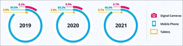
When talking about cameras and photography, especially the casual hobby photography, we cannot ignore the smartphone cameras. According to Rise Above Research reports, smartphones are the most used devices for clicking photographs in the past three years. Smartphone cameras have almost uprooted a segment of compact cameras for casual photography and camera specification has become one of the key considerations for any buyer while selecting a new smartphone. Fig. 1 shows the comparison of number of photos taken with smartphones, digital cameras, and tablets since 2019.
Most important components in a camera
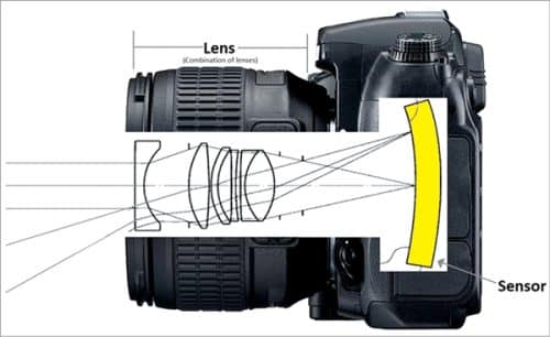
Cameras come in all shapes and sizes. But irrespective of their performance, the digital cameras have three essential parts: A sensor that is the heart of the system, lens or lenses that act as eye(s) of the camera, and the software that converts the analogue data into a usable image. All the three components need to perform well to achieve a good result. But in this article, we are dealing only with the camera sensor.
The camera sensor
A camera sensor is a solid-state device that captures light in small light-sensitive elements called pixels. The sensor detects light as an analogue signal, which is then amplified and converted into a digital signal to store and reproduce later. Sensors cannot produce colours and require a special filter to sense colours.
There are various types of sensors available in the market, such as CCD sensor, CMOS sensor, LiveMOS sensor, or Foveon X3 sensor. The CCD and CMOS sensors are the most common types of sensors in use.
CMOS sensor
Complementary metal oxide semiconductor (CMOS) sensors use rolling shutters and are the most widely used sensors as they can achieve faster data transfer rates (speed) and thus can click pictures at higher frames per second (fps) for a video picture. But as the pixels are read in line-by-line fashion, it causes the rolling-shutter effect. However, CMOS sensors do not produce any smear or blooming effect on the pictures. Further, they have higher dynamic range. But these days CMOS sensors, such as Sony’s IMX661 sensor, also come with a global shutter.
CCD sensor
Charge coupled device (CCD) sensors use a specialised fabrication technology and do not have a conversion electronic circuit on the sensor surface. The absence of electronics from the surface means that CCD can capture more light and have a lower noise factor. Besides, these sensors have higher colour fidelity, making them a better choice in low-light, low-speed use. These sensors feature a global shutter.
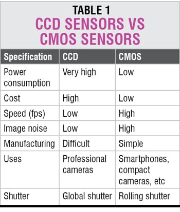
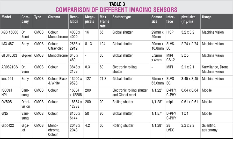
The comparison of CCD sensors with CMOS sensors is given in Table 1.
 Applications
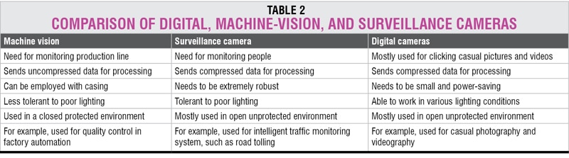
Cameras are used in a variety of applications, including monitoring the movement of people or objects in surveillance systems, such as traffic monitoring systems, drones, etc. Cameras are also used for process automation in factories as a part of machine vision systems, or in automobiles for assisting a driver or enabling self-driving of autonomous vehicles. But the most evident use is in our smartphones for capturing moments.
 Each of these applications have different requirements. A comparison of machine vision camera, surveillance camera, and consumer cameras is given in Table 2.
 Imaging sensor parameters
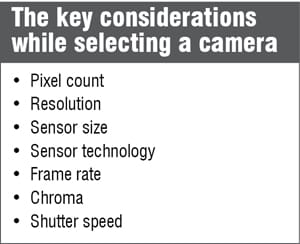
The camera is used in various applications and hence has a lot of different needs and specifications. To understand which imaging sensor is best for our application, we must know some basics about camera sensors. Some important terminologies and technologies are mentioned below.
Pixel and resolution
Before understanding resolution, let us understand what a pixel is. Picture element most commonly known as a pixel is the smallest addressable element of any picture. Pixels are uniformly arranged in a 2D grid to form a picture. The total count of pixels is denoted by megapixels, while the number of pixels in the horizontal and vertical axes determine the resolution of an image.
Resolution in photography means spatial separation and determines the quality of an image. The camera resolution is specified simply by multiplying the pixels available in horizontal and vertical lines within a unit area. Image sensors with higher resolution (more pixels) enable pictures with greater detail and therefore enlargement.
A general rule of thumb is that the sensors with smaller pixels require higher resolution than sensors with larger pixels to achieve the same quality of image. Fig. 3 shows how different resolutions can be compared with each other for similar sized pixels.
Pixel binning
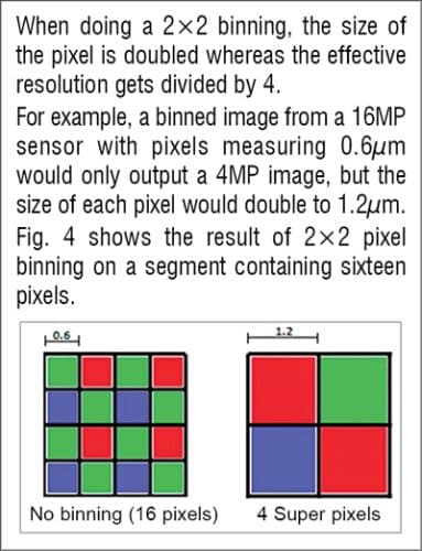
Pixel binning is a technique used to improve the low lighting photography of a portable camera. The quality of image depends on the amount of light captured by the pixels, and larger pixels are better at capturing more light due to their greater surface area. The pixel size is measured in microns.
The latest smartphone cameras are sporting extremely high resolution but with smaller pixel width. The higher resolution works well in bright lighting but sadly not so well in poor lighting conditions. That’s where pixel binning comes into play. Pixel binning is a technique where multiple pixels are combined to form a single larger pixel.
As shown in Fig. 4, sixteen pixels undergo 2×2 binning to create four super pixels. These super pixels will have better balance between brightness and colours.
Devices with very high resolution prefer to use pixel binning. Some smartphones using pixel binning are Redmi Note 10, Google Pixel 6 series, Samsung Galaxy S21, and Xiomi Mi11.
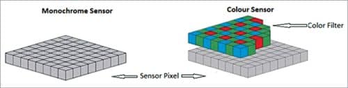
Monochrome and colour sensor
Cameras can detect a wide range of electromagnetic waves. Cameras can be classified into 2 categories, a colour camera and a monochrome camera.
Colour cameras are capable of distinguishing different shades of colours, whereas monochrome cameras can only produce output in different shades of a single colour. As shown in Fig. 5, the colour sensor has an extra layer of colour filter that enables it to capture the colour details. But this filter also reduces the intensity of light falling on the image sensor and thereby slightly reducing the quality of the image. If the application does not require colour detection, a monochrome camera is a better option as it produces better clarity, higher contrast ratio, and does not require any filter.
Global vs rolling shutter
Global shutters were previously available only in CCD sensors, where the whole sensor surface gets exposed to light at the same time, capturing the entire frame at once, which makes it great for high-speed photography. Rolling shutter exposes the sensor in a progressive way, as shown in Fig. 8, which causes images of fast-moving objects to be distorted.
In rolling shutter technology, each row or column of the image is taken one at a time. The readout process of every row (or column) happens in a few microseconds (µs), but due to the very high number of frames, the total readout time for the whole image is in the range of a few milliseconds.
Fig. 6 compares the frame time of the rolling shutter with the global shutter. It can be noticed that the complete frame in the rolling shutter is taken over a period of time, whereas the whole frame in the global shutter is taken at the same time.
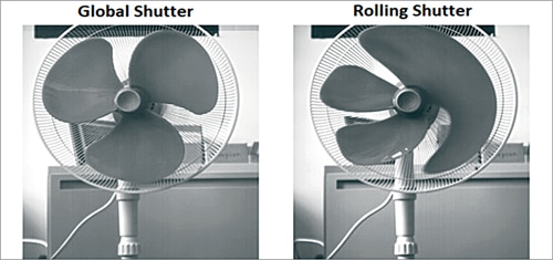
The difference between rolling shutter and global shutter can be understood from Fig. 7. Applications requiring high dynamic range and low noise should employ CCD sensors, whereas applications with faster speed, low power consumption, and tight budget should go for CMOS sensors.
 Frame rate
Frame rate (fps) is the number of images that the sensor can capture and transmit per second. The human brain detects approximately 14 to 16 images per second; the frame rate of a movie is usually 24fps. For fast-moving applications like inspection of newspapers the camera needs to ‘shoot’ in milliseconds. On the other end there are microscopic applications which require low frame rates comparable to the ones of the human eye.
Recently launched imaging sensors
There have been a lot of technical advancements in imaging technologies, and 2021 has witnessed a lot of imaging sensors developed for smartphones, machine vision, etc. Some of the sensors that have brought something new to the imaging technology are mentioned below.
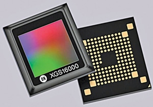
On Semiconductor XGS 16000
On Semiconductors has introduced the new XGS 16000 to its XGS line-up of CMOS image sensors. It is a 16MP sensor with low power consumption of 1W at 65fps. The sensor features a global shutter and has both monochrome and colour options in its line-up. XGS 16000 sports one of the highest resolutions of 4000×4000 pixels for a standard dimension of 29×29mm industrial camera. The use of a standard size makes this sensor compatible with many lenses and camera bodies. It uses the HiSPi output interface for communicating.
The XGS 16000 is ideal for inspection and industrial camera systems, security cameras, and other machine vision application. This sensor being used in Toshiba Teli Corporation’s DDU1607MG/MC is available in an iLGA package that measures 29×29mm. It is ideal for industrial camera systems, inspection systems (food, bottles, recycling labels, etc), security systems, and machine vision camera systems.
SonyIMX 478
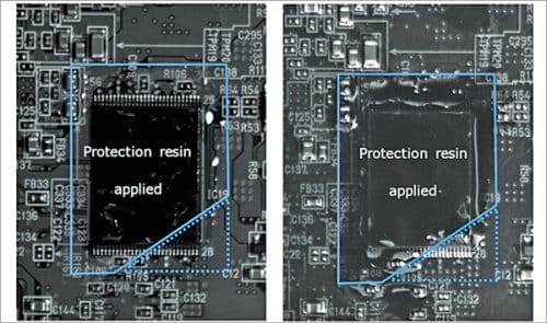
Sony launched the IMX 478 in September 2021. The imaging sensor can take pictures up to 8.13 megapixel with an astounding speed of 194fps. The 1.7cm CMOS image sensor is optimised for UV wavelengths between 200 and 400mm and has one of the smallest pixel size of 2.74×2.74µm currently available in any UV sensor. It features Sony’s Pregius S global shutter, which claims to provide distortion-free image and high-speed performance.
The UV wavelength sensors are widely used in semiconductor industry for pattern defect detection. It is also used for plastic sorting, scratch detection and various other applications. Fig. 10 compares images of the protection resin applied on the substrate line under visible light (left) and UV light (right).
G-Pixel GTOF0503
The GTOF0503 is a CMOS image sensor featuring the indirect Time of Flight (iTOF) technology. The sensor has a resolution of 640×480 pixels, which is around 0.41MP with pixel size of 5µm. It is capable of taking good-quality pictures in challenging light conditions. It uses industry standard MIPI CSI-2 interface, making it a very versatile option. The imaging sensor can be used for 3D mapping, depth sensing, and distance measurement applications thanks to its iTOF technology. It can also be used in vision guided robots, pick and pack robots, etc. Fig. 11 shows the 3D point cloud generated from IR depth map.

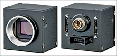
On Semiconductor AR0821CS
The AR0821CS from On Semi was released in the last quarter of 2021. The new 1.5mm CMOS sensor can capture 8.3MP pictures and features a rolling shutter and embedded High Dynamic Range (eHDR) technology. The company claims that it provides best-in-class dynamic range in challenging lightning conditions. This sensor has been used in Basler area scan sensor module daA3840-30mc shown in Fig. 12. The imaging sensor is specially designed for machine vision cameras, drones, scanners, readers, and surveillance systems.
Sony IMX 661
Sony launched the 127MP IMX 661 in the first quarter of 2021. When launched, this sensor had the highest pixel count for any industrial CMOS sensor equipped with a global shutter. This image sensor features an astounding resolution of 13400×9582 pixels with a maximum frame rate 21.8fps . The imaging sensor is quite a lot bigger than any other sensors on the list with its diagonal size measuring 56.73mm. It features multiple exposures, trigger synchronisation, and Pregius Global Shutter technology, which allows the camera to take high-resolution images with very low distortion.
Samsung ISOcell HP1
The ISOcell HP1, launched in the third quarter of 2021, is the industry’s earliest 200MP sensor specially developed for handheld devices, such as smartphones. This sensor features a small pixel of 0.64µm and employs Chameleon Cell pixel-binning technology. Depending on the ambient lighting, Chameleon pixel-binning can capture full resolution pics or employ a 2×2 pixel binning with an output of 50MP picture, or even 4×4 binning to provide a 12MP image in extremely low-light conditions. The sensor can capture 8k videos at 30fps and can deliver data at rate up to 4.5Gbps per lane using D-PHY interface.
Samsung GN5
Samsung launched the GN5 imaging sensor alongside the HP1 in the first week of September 2021. It is a 50MP sensor with extremely fast autofocusing capabilities. Samsung claims that the GN5 is the industry’s first 1.0µm sensor with a Dual Pixel Pro technology, which can place dual photodiodes and recognise pattern changes in all directions to enable an all directional autofocusing. It also has Samsung’s proprietary pixel technology. Samsung claims that with these two technologies the sensor can instantaneous autofocus even in extreme lightning conditions.
Omnivision OVB0B
In January 2022, Omnivision launched its first 200MP camera sensor, which claims to have the smallest pixel measuring just 0.61µm×0.61µm. For superfast autofocus, it employs 100% Quad Phase Detection (QPD), which also makes it the first 200MP sensor to offer this feature. Like Samsung’s HP1, it also features a 4×4 pixel binning to provide an output of 12.5MP at 30fps with 3-exposure staggered HDR timing. The sensor supports CPHY, DPHY, and dual DOVDD for interfacing.
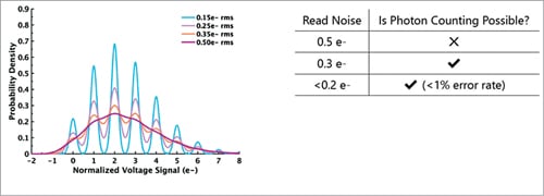
Gigajot Gj00422
Gigajot has released the Gj00422, a photon counting, Quanta Image Sensor (QIS). This is the first sensor capable of photon counting at room temperatures at full speed while achieving full high dynamic range. The Gj00422 is a 4MP sensor with square pixels measuring 2.2µm. Unlike the traditional CMOS sensor, where numerous photons are collected inside a pixel well and converted into electrons, QIS operates by detecting individual pixels in order to work in a poor-light environment with much higher fidelity than other types of CMOS sensors. It also features an on-chip temperature sensor and high intra-scene dynamic range. This sensor is suitable for astronomy, medical, industrial, defence, and other high-performance applications.
Future of imaging sensors
The camera technology has come a long way, and the advancement does not seem to be slowing down any time soon. The improvement in SSD devices means that higher resolution in smaller-size sensors is a safe bet to place.
Recently, researchers from Princeton University were able to fabricate a camera the size of a salt grain that can capture high-quality images, which means that the size of imaging sensors can be reduced to unperceivable sizes.
 With the growth number of individual content creators, smartphone manufacturers are forced to improve the cameras in their devices. Many smartphone manufacturers are planning to use a bigger 2.5cm (one-inch) sensor, artificial intelligence, and high-quality lenses to improve camera capabilities. But only time will reveal how cameras improve in the coming years.
The author, Sharad Bhowmick, works as a Technology Journalist at EFY. He is passionate about power electronics and energy storage technologies. He wants to help achieve the goal of a carbon neutral world.
