


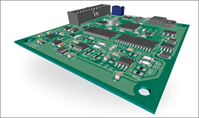
The electronics industry is expanding like never before. But every application is dependent on that tiny block called printed circuit board (PCB), which is totally hidden by wires and connected devices. The next time you start a project, why not design your own PCB, instead of getting someone else to do it for you? Here is how you can do it with DipTrace.
DipTrace is a PCB designing software that helps you design a neat and tidy board that works as per your needs. But when so many such software are available why should you choose to go with this specific tool? Let us try to find an answer to this question by looking at what the software offers for every stage of designing.

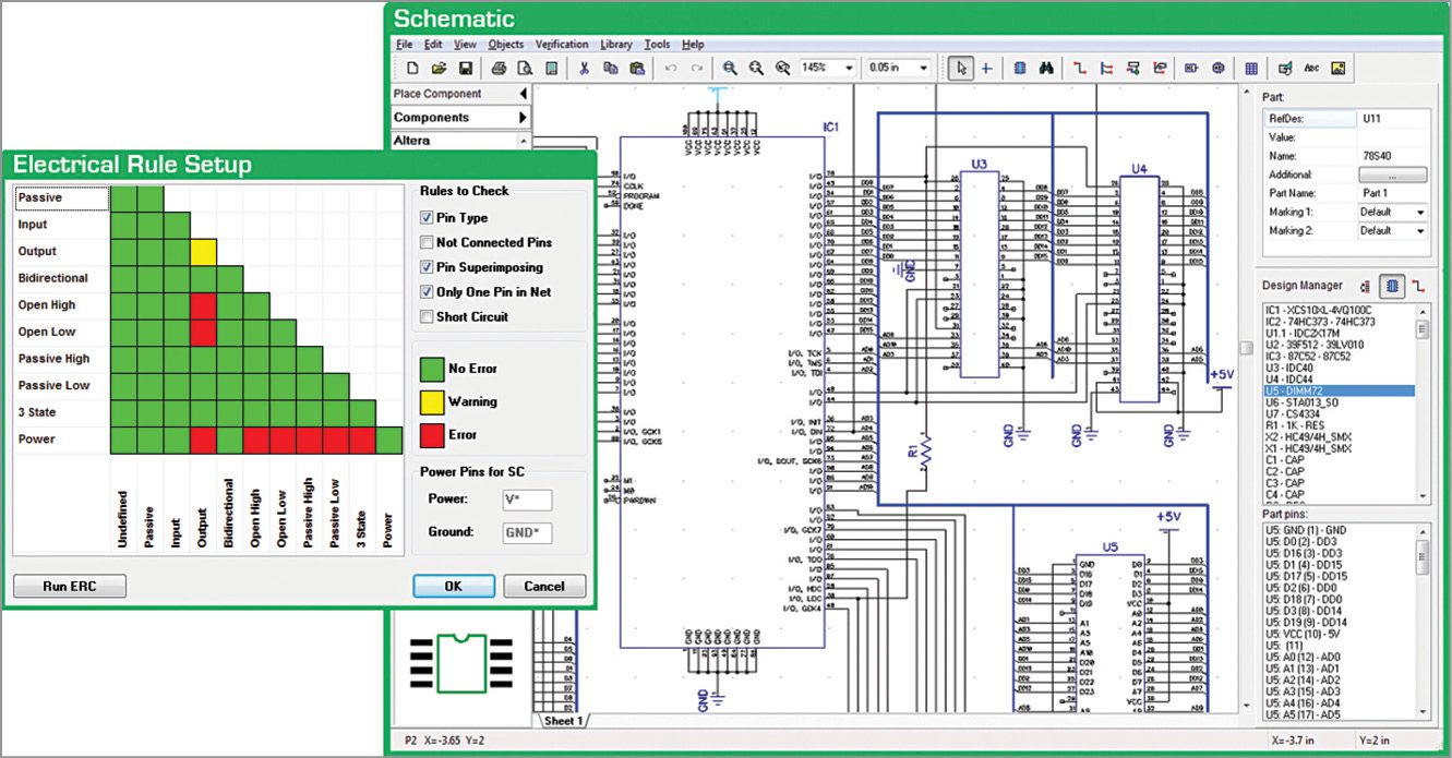
Easier sub-section design. While designing a circuit, it is always comfortable to make small parts that you know would work for sure and then piece these together to form the complete circuit. But this is not as easy as it seems, as there are complications with making sure the signals flow correctly and with ensuring common ground connections.
You will find this problem easier to handle in DipTrace, where each sub-section can be designed on a separate sheet. The first sheet becomes the face of your design, to which the others can be linked hierarchically using connectors between sheets.
For nodes like power supplies or repeated ones in the design, you simply have to connect the nets to the same net port. The nets are then automatically linked across sheets, without wires. You can simply use a bus connection for groups of wires that go together. Nets on different sheets are connected by names, while buses on different sheets have exclusive connectors.

Once the schematic is complete, DipTrace allows you to cross-check parameters you might have missed, like shorts, or to super-impose pins by an electrical rule check (ERC) that is flexible in allowing you to choose the features you want to verify.
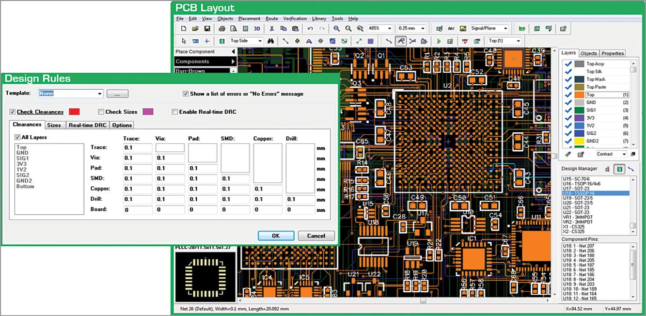
Pick and place your layout. Moving from the schematic design to the PCB layout stage, you can take forward the same schematic rules or import design rules from an earlier project. On importing non-schematic rules, your PCB is ready with net classes, layers and design constraints.
One of the major issues in creating layouts is the size: whether it will fit within the board it has to be printed on. This process is smooth with DipTrace, which lets you first draw a board outline in the required shape, manually pick and place whatever parts need to be fixed and then auto-place the rest. You can then add connections and fiddle around with your design to get the right component-connected layout.
Make the most of a customisable auto-router. Before you can begin routing your design, layers, via styles and net classes need your attention. These form the foundation of your board design, and with DipTrace you can customise and group your settings. The tool gives you the freedom to decide what signals should pass through which layer, choose colours, specify hole dimensions and manage via styles and net classes.
You can then decide how the auto-router should work, thus exercising complete control over your design, effortlessly. At any stage, you may save the settings in a rules file to use in a future project.
If you are going with the auto-router for routing your wires, there are grid based and advanced shape based options. You can set it up to work the way you want and it will automatically take care of your requirements.
If you choose to do it manually, you can select from available modes and, as you route, the tool warns you of design consistency errors. Thus, you take care of the design errors as you move along. You can always edit your work and even move nets between layers.
Remaining free spaces can use the copper-pour facility for low-impedance connections and additional heat-sinking. DipTrace allows you to organise different copper pours on a single layer, as well as connecting copper polygons on different layers into a single net.
A detailed procedure is available to verify the design. This includes checking for design rules and net connectivity. With errors shown at the exact location and different types marked in different colours, rectifying these becomes easy.
Relate the schematic and the layout. While completing your layout is important, it is as important to ensure that the schematic and the layout are in sync. There might be cases when you have to add components after the layout has been designed. With compare-to-schematic, renew-design-from-schematic and back-annotation features, this procedure is relatively simplified.
Export for manufacturing. Gerber files for printing PCBs can be exported layer-by-layer or in batches with DipTrace. You can even specify details like what components need to be exported to the files, what accuracy is needed and preview to visualise your configuration.
Numerical control (N/C) drill file that needs to be sent in to the manufacturer can also be generated with just a few clicks. Also, with 3D-preview-&-export module, you can see the 3D model of the board with all components installed, rotate it, change parameters to see the effect and export 3D PCB in STEP format for mechanical computer-aided design integration.
Efficient and easy to use
Having seen how you can use DipTrace to design PCBs faster and better, one might wonder how the tool manages to do what it does. Let us now take a look at three features that make the design tool work its magic.
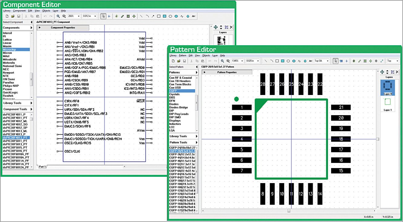
Component editor. Manage component library, make new components and edit old ones with this editor. You can design the component, choose its properties and functioning details.
For chips, you have the choice of different kinds of packages, too. You can even group pins based on their functionality and handle these as a single unit.
Pattern editor. Every component has a particular pattern (footprint) on the PCB on which it is placed. This is like the allotted place with required connections in order. This editor helps you make and edit these patterns, letting you specify the parameters. Pad specifications like position, shape and numbering can also be worked around using templates and special features.

Pattern editor also allows you to connect patterns to your 3D model for a wholesome picture.
Cross-module library management. With exclusive sections for components, patterns and 3D models, all libraries in DipTrace are organised into groups where both components and patterns can be stored. The structure of the libraries gives easy access to components. Also, with an efficient filter, you can search these by reference, designator, type or value.
Learn from first-hand experience
There are two factors that seem to be making users choose DipTrace. One is the graphical user interface (GUI) that is easy to use, easy to learn, intuitive and familiar. The other factor is export/import feasibility.
The process adds no complications and thus, users find DipTrace easy to work with when they want to use multiple software for different areas of expertise, like exporting files to Spectre for auto-routing.
There are also users who stick to the software as developers are active on various forums. Certainly makes it easy when you have doubts you want answered quickly, would you not say?
Interestingly, you can install DipTrace on multiple systems, but only one copy of the software should run at a time. A user on Parallax forum says, “I use DipTrace but also use Eagle to review designs for customers that use Eagle. I would definitely say that DipTrace is better of the two. I still struggle with certain things in Eagle, but DipTrace was easy to use from the get-go. I am still learning all the tricks, but throwing together a basic PCB in DipTrace is super easy and requires very few intelligence quotient points.”
DipTrace developers are open to user complaints and appropriately react to the engineering community with improvements and updates.
Make the most of updates
DipTrace enjoys huge community support and offers good support to its users. The version with this month’s DVD is DipTrace 2.4. Get accustomed to it quickly as the next version 2.9 is in Beta stage. It includes support for differential-pair routing, not just in designating nets as pairs but using it as a single unit while routing manually.
An interesting way of working with this tool is to use hot-keys or keyboard shortcuts. The latest version allows you to customise your hot-keys according to your comfort. With additional support to the modern open database (ODB++) and new-generation Gerber X2 formats, PCB manufacturing seems to be at its best.
The author is a technical journalist at EFY
