


 A high input impedance AC and DC active probe is required to increase the input resistance and sensitivity of such measuring instruments as oscilloscopes and multimeters. Presented here is one such solution that consists of a single operational amplifier (op-amp) and selectable gain. The active probe protects inputs of the test equipment during testing and experimentation. The probe can easily connect to and disconnect from other equipment.
Circuit and working
The circuit diagram of the simple AC and DC active probe with high input impedance and selectable gain is shown in Fig. 1. It is built around an op-amp TL071(IC1) and a few other components.
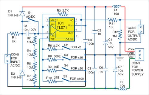
The circuit is designed for a single op-amp with a stable gain of +1 and low input current (JFET inputs). It is capable of driving at least 600-ohm load. Op-amps like OPA132, OPA134, TLE2071 and TLE2081 may be used here. You may also use MCP601, but the power supply should be ±3V. In fact, you can use a large variety of op-amps with JFET inputs, including the classical TL061, TL071, TL081, LF356, LF357 and so on, with slight modifications including resistors, capacitors and corresponding power supplies.

Switch S1 is closed for DC input signals and it is open when you wish to work only with AC input signals.
To make it simple and compact, the probe does not use a multi-trimmer potentiometer or any additional components for adjusting offset of the op-amp. Including offset is not a big issue; it can be done at the output of the probe. Usually, offset does not change much if you use an regulated low-noise power supply and ambient temperature does not change a lot.
Input resistance
Input resistance of the probe is set to 40-mega-ohm using resistors R2, R4, R5 and R7. Such high input impedance makes the probe appropriate for examining signal sources with high internal resistance and with low level of output signals.
Selecting the gain
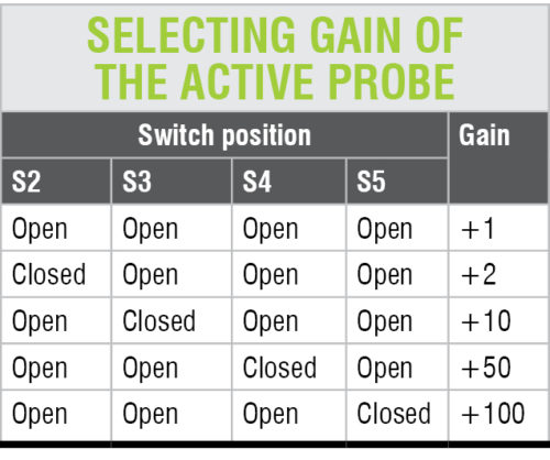
The probe does not need any adjustment to work properly. Before using the probe, set the position of S1 (AC or DC input) and the gain (close one of the switches from S2 to S5). Gain of the active probe is set with the four switches S2 through S5, as described in the table. Bandwidth depends on the actual op-amp used.
It is preferable to select resistors R3, R6, R8 to R10 from E96 series. You can change the gain to any appropriate value as per requirement.
Power supplies
This circuit requires two power supplies: positive terminal at pin 7 and negative terminal at pin 4 of IC1. Depending on the op-amp used, you may use power supplies as 2x 3V, 2x 3.3V, 2x 4.5V, 2x 5V, 2x 9V (two 6F22 batteries), etc.
Also, depending on the op-amp, the active probe can have low power supply current (for example, MCP601 or similar op-amp), so the battery will work hundreds of hours without requiring to be replaced. Depending on the op-amp and the required amplitude of the output signal, power supplies can be from ±3V for MCP601, to ±18V for OPA132 and OPA134.
Power supplies are filtered with LC filters to reduce the noise introduced by external power supplies working from AC mains or from DC/DC converters.
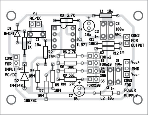
Construction and testing
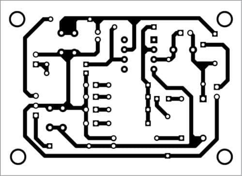
A PCB layout of the active probe is shown in Fig. 2 and its components layout in Fig. 3. Assemble the circuit on the PCB. Connect AC/DC input across CON1, so output is available at CON2.
Download PCB and Component Layout PDFs: click here
Connect the dual-power supply depending on your requirement. Alternatively, you can use two 9V batteries (6F22) as the dual-power supply.
The circuit can be used as a universal high-impedance buffer with selectable gain. Care should be taken while using the probe because the high input resistance of the probe can capture a lot of electromagnetic noise.
EFY note
The circuit and PCB are designed for op-amp TL071 or equivalent op-amp. If another op-amp is used, modify it accordingly.
Petre Tzv Petrov was a researcher and assistant professor in Technical University of Sofia, Bulgaria and expert-lecturer in OFPPT (Casablanca), Kingdom of Morocco. Now, he is working as an electronics engineer in the private sector in Bulgaria.
