


The fact that a component is mounted on a board does not necessarily reduce its ability to be imaged and checked with ultrasound. Here is how it can be done.
As they progress from raw materials to ready-to-mount devices, electronic components encounter various mechanical and thermal stresses. These stresses are capable of initiating internal structural anomalies such as cracks, non-bonds, and delaminations.
Such anomalies threaten the long-term performance of a component and of the system in which it has been installed. Assemblers try hard to identify suspect and defective components and remove them before they are mounted onto circuit boards. The mounting process itself can also be cause for concern because the components are subjected to mechanical and thermal stresses that can induce defects in components that were defect-free.
Structural anomalies can be found without harming the component package by using high-frequency ultrasound imaging to ‘look inside it.’ In this process, focused pulses enter the surface of the component and echoes return from internal interfaces. As a pulse travels through a component, these events may occur:
- When the pulse strikes an interface between two bonded solids, a predictable portion of energy is reflected back to the transducer. The other portion goes deeper into the component.
- As the pulse travels through a homogeneous material, no echoes are generated.
- If the pulse strikes an air gap, almost all of it is reflected. None crosses the interface because ultrasound at these frequencies does not travel through air.
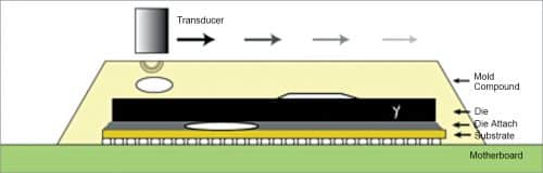
An acoustic micro imaging tool, such as a Nordson SONOSCAN C-mode Scanning Acoustic Microscope (C-SAM), scans over the area of the part, produces the pulses, collects the echoes, and assembles the data into an image. The tool’s transducer is immersed in water to couple the ultrasound to the top surface of the component. The transducer moves swiftly back and forth across the part and pulses ultrasound at up to 25,000 x-y locations per second, receiving the echo from one pulse before launching the next pulse. Frequently, components are screened in trays to identify for removal those with internal defects, but components mounted on boards—the subject here—can be imaged after reflow to look for defects.
The amplitude of an echo carries information about the interface from which it came, and this is used to assign a specific colour to its pixel. Usually, the operator of the tool does not attempt to image the entire thickness of the component, but only the depths of interest.
If all the echoes in the acoustic image correspond to known internal interfaces in x-y location and amplitude, the part is judged to have no defects. If there are features in the acoustic image caused by echoes from unexpected interfaces, the part may have an anomaly.
Fig. 1 shows four of the anomaly types that may be found when a single boardmounted BGA package is scanned. All four types are gaps that contain air. Each has a solid-to-air interface that reflects nearly all the arriving ultrasound.
The white oval at the upper left is an isolated void in the mould compound. It is a fairly large bubble of air, but its potential for causing damage is likely small because it is not near wires or other key items. It is unlikely to expand in size. It is discussed separately below.
The white feature in the die attach material is a risk because it will block heat radiating from the die and could cause the die to overheat and fail. It might also expand because it is close to two solid surfaces having different thermal expansion characteristics.
The third feature is not a bubble-like void but a delamination between the mould compound and the die. Delaminations can be only a few microns thick; the thickness of the delamination shown here was exaggerated to make it visible.
The fourth feature at the right end of the die is a crack. Thermal and mechanical stresses make it very likely that an internal crack like this will damage the circuitry above.
The area surrounding the void in Fig. 1 is shown in more detail in Fig. 2. The scanning transducer that pulses ultrasound into the part is out of sight above the part. The leftmost arrow represents a pulse arriving from the transducer and striking the mould compound-to-air interface at the centre of the void. Because the interface at this x-y location is horizontal, virtually all of the pulse is sent back to the transducer as a high-amplitude echo.

The second pulse strikes an angled interface, and much of it is scattered in directions away from the transducer. The percentage of the pulse reflected to the transducer depends on the location of the point of reflection on the downward sloping interface. Some of the echoes will reach the transducer but will be imaged in a colour such as blue.
The third pulse misses the void and strikes the interface between the mould compound and the die. The interface between these two solids reflects about 60% of the pulse to the transducer. The remaining 40% of the pulse travels into the die and will be reflected from the next material interface it encounters.
What the diagram does not show is the amount of data that is collected by scanning. If the void is 1mm wide, the number of x-y locations from which echoes are received during a single pass across the void approaches 100, but may be more if higher resolution is required. The speed with which ultrasound travels through production materials is typically very high. As the transducer is scanning, the first pulse to encounter the void will send back an echo and the echo will be received.
The next x-y location in line will not be pulsed until after an interval. The transducer will collect echoes from all x-y locations where there are material interfaces.
In the BGA package in Fig. 1, the interfaces at the top and bottom of the die are key defect sites. The same is also largely true of other package types, such as the two QFPs shown in the following figures.
Fig. 3 shows one region of a printed circuit board, which was first imaged optically in black and white. The two largest components were then scanned individually by a C-SAM acoustic micro imaging tool, and the acoustic images were then superimposed on their optical images in this figure. Colour in the acoustic images is determined by the amplitude and polarity of the return echoes.
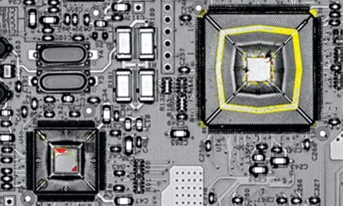
As long as it can be accessed by the acoustic tool’s transducer, any flat item on a printed circuit board can be imaged. For example, the numerous large and small ceramic chip capacitors in Fig. 3 could be imaged to find internal cracks or voids. The AMI tool is programmed to recognise each board type, and can navigate to accommodate components of varying thicknesses.
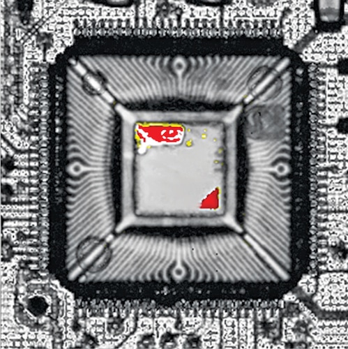
Fig. 4 is the acoustic image of the lower left IC package in Fig. 2. The items of interest are the two red features at the corners of the die; white regions are similar but a bit more highly reflective. Both features are air-filled delaminations between the overlying mould compound and the surface of the die. A delamination on a die face, even though it may be extremely thin, has two unfortunate characteristics: It is very likely to grow in area as a result of thermal cycling over time, and it can easily shear off wire bonds that it encounters as it grows.
The die region of the larger IC package is shown in Fig. 4. This image was gated on the die surface—meaning that only echoes whose arrival time indicated that they had originated within a vertically narrow gate encompassing the die surface were used. Gates can be made very thin, if needed, and are used to avoid depth confusion among features, as well as to determine the precise depth of a single interface.
Fig. 4 displays numerous yellow, red, and white features, which are mostly associated with the perimeter of the die—meaning that the features are close to the vulnerable wire bonds. All of the anomalies can be classified as delaminations or voids. Red and white indicate the highest degree of reflection, while yellow indicates somewhat lower reflection, probably because the top surface of the anomaly is slanted rather than flat and thus directs some of the echo away from the transducer.
Some of the peripheral features may be harmless, but there are three red-on-white features on the die itself that are not. These are the one at the lower right corner of the die, the one at the upper right corner, and the one about a third of the way up the left margin of the die. Each of these is in contact with the die surface and is capable of expanding its area and cleaving wire bonds—or may already have done so.
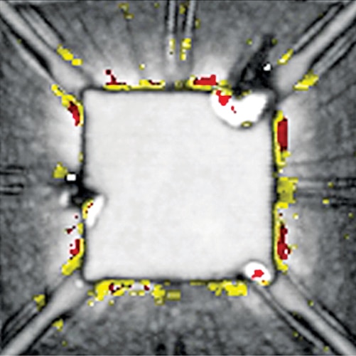
The large defect at the upper right corner appears to have a large, somewhat indistinct black area attached to it. This is almost certainly an extension of the void (which may actually be a crack) upward toward the surface of the mould compound. The transducer is collecting only those echoes whose arrival time matches the narrow gate enclosing the die surface. If this extension of the defect extends upward above the top of the gate, the x-y region corresponding to the extension will send no return echoes and system software will fill that region with black pixels, meaning no signal received from within this gate.
The defect along the left edge of the die has a similar black region associated with it, and probably of similar origin.
One important post-reflow evaluation of mounted components uses ultrasound to measure rather than to image. Suppose a new lot of a particular component is being mounted—a component that has a solid history of few failures. The new lot, however, has abundant defects, and production halts. The acoustic micro imaging tool can measure the acoustic impedance of the mould compound on the new components and on samples of previous components. If there are significant differences between the two, it often means that the composition of the mould compound, and hence its response to the stresses of handling and reflow, has been altered by the manufacturer.
The images shown here were made with C-mode imaging, where the amplitude and polarity of each returning echo is assigned a colour. Numerous other C-SAM imaging modes can be used on mounted components to make, for example, a nondestructive cross-section through a component. Internal features, including defects, can also be imaged by two types of acoustic 3D imaging modes. The fact that a component is mounted on a board does not necessarily reduce its ability to be imaged with ultrasound.
Tom Adams is a consultant to Nordson SONOSCAN
