
The effects of electrostatic discharge and interference is often ignored by designers, which results in their rejection, especially in global markets. The designers need to take care of such international standards as FCC, CE, and VCCI if they want their products to succeed in international markets. This article explains the causes of failure as well as the remedies.
EMI stands for electromagnetic interference, EMC for electromagnetic compliance, and ESD for electrostatic discharge. These acronyms define how a product can unintentionally become a source of radio frequency waves generation, or how it can become a victim of radio frequency waves that come from various sources in the environment.
ESD defines how robust a product is to withstand the static voltage discharge that is accumulated by the human operator. Standard bodies like FCC (Federal Communication Commission) in the USA, CE (Conformitè Europëenne) in Europe, and VCCI (Voluntary Control Council for Interference) in Japan specify the amount of radiation an electronic product can radiate, or the amount of radiation an electronic product should withstand without any permanent failure. Similarly, there are voltage discharge levels that a product should withstand without getting damaged.

With increased use of electronics in our daily life, compliance to these standards ensures that the users are safe and products do not pollute and affect the working of products in the vicinity. While each country has its own standards, they do not vary much in values.
However, from the electronic packaging point of view we need to know what standards the products should meet. Knowing the standards helps in designing the packaging such that the products meet the required standards. The best strategy is to get the worst-case limits and design the product for them. However, cost of doing this may be high in some cases.
Let us understand the basics of the radiation mechanism for designing a compliant product. Almost all electronic products radiate or get impacted in either of the two modes. These are:
Conducted emission (CE)
Power and other cables act as carrier and radiate unwanted RF signals.
Radiated emission (RE)
Product itself radiates, like an RF transmitter.
The frequency limits for conducted and radiated emissions are different. Most emissions are radiated emissions, and these are spread over large bandwidths.
Radiated emission requires an RF transmitter and a receiver for energy transfer. Typically, during testing, the transmitter would be the product under test and the receiver would be a spectrum analyser fitted with an antenna to measure strength of the RF energy. Fig. 1 shows the radiated and conducted emission mechanism in a product for our understanding.
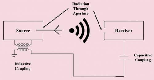
But most radiated emissions are through apertures (such as ventilation holes, corner seams, and gaps between the chassis bottom and top) in the enclosure in addition to cables (power and signal) that add to the overall radiation. While power cable radiation is measured as CE radiation due to signal cables, it is a part of the total radiated emission.
This is one reason why products with large cable connections (Ethernet switch cables, sensor cables, etc) have to be designed carefully and any source of radiation has to be contained within the enclosure, as managing cable radiation can be challenging and expensive.
For validation of a product’s compliance, it is kept in an anechoic chamber and an antenna is kept at a designated distance from the product (three metres or ten metres) depending on the standards to which the product should comply. The antenna is connected to a spectrum analyser through proper instrumentation to measure level of signal radiating from the product for RE measurement. The reading is mapped against the level specified by the standards. If the signal level is lower than the specified level, the product is certified for compliance.
In case of conducted emission, power cable of product under test is connected through a line impedance stabilisation network (LISN) to spectrum analyser and the signal levels are measured and, as in case of radiated emission, mapped against the standard specified values. Fig. 2 and Fig. 3 show the radiated and conducted emission levels of FCC and EU standards mapped for understanding the standards better.
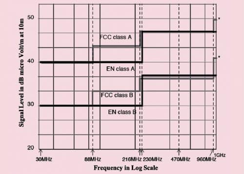
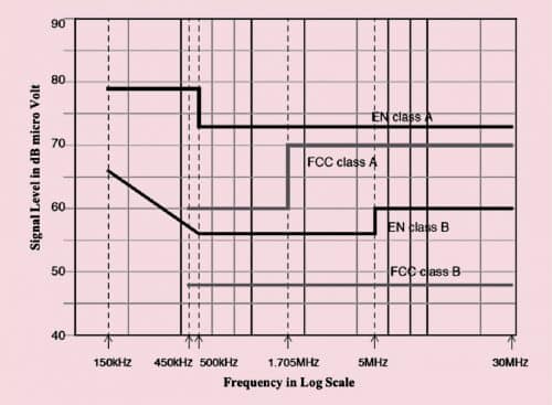
The standards define two sets of levels called Class A and Class B. Table 1 shows the applicability of the classes in the USA and EU.
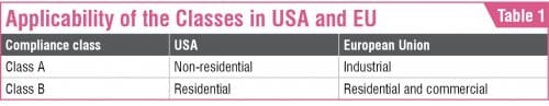
Class A allows higher radiation as industrial environment is very noisy. However, Class B has much lower (stricter) radiation limit and most consumer goods need to meet this standard.
A note of caution
Designers think EMC and EMI problems are due to enclosures alone. This is a myth every designer should be aware of. For a successful compliance, the entire product has to be designed to meet the standards. PCB assemblies (PCBAs) are the major culprits and these need careful EMC/EMI design in addition to enclosures.
Solutions for radiated and conducted emission vary in implementation. Primary details needed are the frequencies at which the electronics of the system operates and the RF carrier frequency if the product is a radio equipment. Basic square waves tend to contain harmonics, which contribute to the radiation in a big way. A solution to radiated emission is reduction in emissions from the PCBA, which basically depends on the circuit design.
Experience shows high-speed digital circuits are the main sources for radiation as these have square waves with small rise time.
Circuit design for EMC/EMI reduction is a vast topic and is not being covered here as our primary focus is on electronic packaging. However, radiations from PCBAs can only be reduced and cannot be eliminated fully, and that job has to be done by the enclosure and filters.
The process of containing RF radiation is called shielding. Metals are the best shields to contain radiated emission. So, in case of a product with plastic enclosure RF radiation containment can be a big issue. Even metal enclosures having imperfect joints, seams, or ventilation holes can be a source of RF radiation. In case of fastening mechanism of enclosures like rivets and simple screws, the space between two screws/rivets can also become a source of radiation. This is the reason why designers have to understand the compliance needs up front (SCoPE framework) to decide on the enclosure joining/fastening mechanisms.
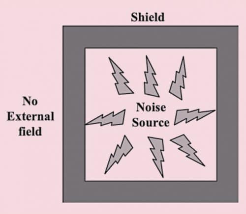
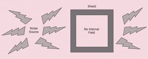
Before getting further into the solutions for radiated and conducted emission let us understand the mechanism of shielding. Fig. 4 shows an electronics system inside a shielded enclosure with no external field. Due to the shielding no radiation escapes (radiated emission prevention). Fig. 5 shows the exact opposite where the shield prevents the radiation from entering and the system inside the enclosure is not impacted (radiated emission susceptibility) by the external radiation.
Metals are the best shielding materials due to their conduction property and therefore metal enclosures are found good for EMC/EMI protection. Plastics are bad for shielding as RF waves pass through plastics. Shielding effectiveness of a metal depends on its thickness and the frequency of RF emission. But, as a rule of thumb, mild steel has good shielding characteristics as compared to aluminium.
As we saw in Fig. 4 and Fig. 5, an ideal shield would be a tightly closed box for best performance. However, in real life, any enclosure will have seams (due to sheet-metal design) and openings for displays, switches, and cables. From a radiation perspective these are called apertures. Apertures in an enclosure lead to leakages of RF radiation. The best EMC/EMI performance is achieved when these radiation leakages are reduced to a low level.
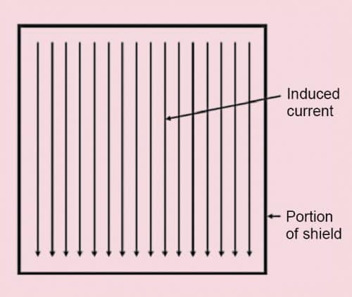
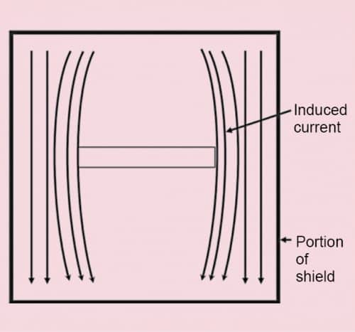
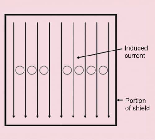
Normally, noise fields (created by RF radiation) induce currents in the shields and these currents induce additional fields in the shield. These new fields cancel the original fields in some spaces. For this cancellation to occur, the shield currents must be allowed to flow without any hindrance. Fig. 6 shows how the induced current flows when there are no apertures and Fig. 7 shows how the current flow gets disturbed when there is an aperture.
We need to remember that most electronic systems need ventilation slots for heat dissipation, which can be a problem for the EMC/EMI. One of the solutions is to provide the ventilation through a cluster of holes, which allows the induced current flow undisturbed as shown in Fig. 8.
Another challenge in enclosures are the seams. Seams are inevitable in sheet-metal enclosures as the enclosures are made of multiple sections. When the sections are fastened by rivets or screws they make the seams leaky due to apertures. If these seams have to be made leak-proof three things need to be done:
- The adjoining sections should overlap.
- The rivets and screws should be as close as possible to reduce the aperture effect. This is where welding helps!
- The two overlapping surfaces have to be conductive and, for better shielding, EMI gaskets or EMI fingers should be used.
A challenge that designers face in electronic packaging very often is that a solution to one problem leads to another problem (EMI/EMC vs heat dissipation). However, sheet-metal enclosures lend themselves to EMC/EMI problem in a natural way, while plastic enclosures pose a big challenge for EMC/EMI.
To make plastic enclosures meet EMC/EMI needs these have to be made conductive. Most popular but expensive solution is to coat a conductive paint inside the plastic enclosure, or to make the plastic conductive with additives. Other methods are electroless plating or metal-foil lining, both of which are expensive and delicate.
Another approach is to enclose the PCB assembly in a metal shield so that the plastic enclosure does not have to be treated for EMC/EMI. This approach is popular in radio products as sometimes power levels are high and need to be contained in the PCBA module itself. PCB-mounted shielding can be custom designed, or ready-to-use shields can be tried. Most Wi-Fi and Bluetooth modules come with shields to reduce extraneous radiation and their PCBA is shielded, except the antenna.
The best way to make a product EMC/EMI-standards compliant is by following the six-step process mentioned below:
- Understand the standards compliance needs with respect to radiation and budget 3dB more for safety margin. Just meeting the limit is perfectly fine with certification process but due to manufacturing process there may be variations, which can fail the product.
- Ensure the enclosure is well designed, keeping the above-mentioned information in mind. But if off-the-shelf enclosure is being used, ensure right enclosure is chosen. More than the selection, follow the process recommended by the vendor for assembly. (I remember we had used an on-PCB shield as EMI solution and the product passed the limits with good margin. However, during production we found the products failing sample tests. We walked through the production line and found that the stage where on-PCB shield was being installed had an issue. Due to margin error in the holes in PCB the shield could not be inserted easily, and the technician was pushing the shield in using a nylon mallet. It was a perfect way to do, but the mild nylon mallet blow opened up the shield’s seam on the sides and lead to radiation failure! In case of FCC certification, when you get an FCC registration number for compliance, it intrinsically means that FCC can take samples from the market and test your product for radiation compliance. So, EMC/EMI certification is a fairly intense job.)
- Electronics circuit design and PCB layout as per design guidelines is important but fairly intense and cannot be covered here.
- First version of the product should be subjected to a pre-scan in a lab to get the measurements. This will give a telltale story of the product in its current form. Solution can be implemented without much time and effort in the next revision.
- When the scan (both pre and final) is done by rotating the product 360° around vertical Y axis, the reading shows up any seam- or aperture-related leakages. Some labs do it in a static way with product rotated 90 degrees on its four sides. This can sometimes mask the radiation issue, so it is better to do the scan with a rotating table.
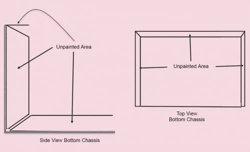
- From the reading the source of radiation leakage can be identified. A normal spectrum analyser reading will have frequency on the X axis and radiation level on the Y axis; angle has to be manually observed by the compliance engineer and design engineer. Designs based on sheet-metal enclosures can fail due to fabrication and design mistakes like gaps in corner bends from where radiation can leak. The best solution is to have an overlap between top and bottom of the sheet-metal enclosure, which also has to be conductive (no painting/coating) with un-painted overlaps. Fig. 9 shows cross-sections of an enclosure for better understanding.
Electrostatic discharge
Electrostatic discharge occurs when 10-15kV charges accumulated on a person or object get discharged through the electronic product. The ESD damages the semiconductors permanently. Its effect is high when the atmosphere has less humidity, but it can never be avoided. Unless protection measures are taken, the product can get damaged very easily and silently. There are two ways to protect a product from ESD:
- Provide ESD protection at inputs of the semiconductors that are exposed to the outside world. These inputs are typically connectors, which calls for circuit design with proper ESD protection. The protection devices are called transient voltage suppressors. These reduce the ESD to a safe level, preventing damage to the semiconductors.
- Ensure the enclosure has no gaps through which ESD can sneak and the enclosure is grounded properly to act as an excellent ESD shield. While metal enclosures have a good ESD shielding capacity, plastic cabinets are not so lucky. Irony is plastic cabinets are also poor in protection against EMC/EMI and shielding internally is critical for the safety of a product.
Normally, good EMC/EMI countermeasures should work for ESD too in most cases. However, improper grounding in the mains supply can sometimes make the product a victim to ESD. A successful method to prevent PCBAs from getting damaged by ESD is to provide copper trace of 1-2mm width around the edge of the PCB. (The trace end should not be connected to form a loop; it should be open and one end should be connected to chassis ground.) Other candidates that attract ESD are the exposed connector pins (especially berg sticks). The in-circuit programming connectors for the microcontroller programming normally are the culprits. These measures help in ESD voltages being diverted to the grounded trace instead of damaging the semiconductors.
Most of the times ESD solution can be implemented only after the testing of the product has been done after taking all precautions during its designing. ESD standards, however, do allow a system to restart after the start in some applications. But restarts are not possible in mission-critical domains like medical, avionics, and some industrial equipment.
The author has 35 years of design experience for various domains and global customers. This article is based on the last chapter in his book titled ‘Introduction to Electronic Packaging – Unconvetional Guide to Product Design.’