


When power is applied, an integrated circuit begins to heat up within its package. It shortly reaches the operating temperature range for which it was designed. Excess heat begins to dissipate along a path designed for the die. If there are no structural anomalies along this path, heat dissipation from the IC will be uneventful.
For a low-power IC packaged in plastic and mounted to a printed wiring board, the dissipation path may be very simple: heat flows downward through the die attach and further dissipates through the metal die paddle. From here it makes its way through the backside mould compound. If the level of heat dissipated is low, heat-blocking anomalies along this path (die attach voids and non-bonds, for example) may have little effect, unless these cover a significant area of the dissipation path. But for higher-power dies, the absence of structural anomalies along the path is more critical and the path may terminate in a metal heat-sink designed to dissipate the higher heat flow.
The task for assemblers is to ensure that every die has a clear heat dissipation path. This means paying attention to die attach voids and surface contamination that can lead to non-bonds. For example, in plastic IC packages gaps may also occur in the bond between the backside of the die paddle and the mould compound. In insulated-gate bipolar transistor (IGBT) modules, even if no voids or other gaps are present, heat dissipation can be impaired by the tilting or warping of one or more interfaces along the dissipation path.

Die failures from imperfect heat dissipation can, to some degree, be anticipated by destructive physical analysis of field failures and of assemblies that have been life tested. These results may point to a process step that needs to be altered, or to a material that needs to be modified. A more direct method for finding structural anomalies is an acoustic micro imaging tool, which non-destructively images and analyses internal structural features, including voids, non-bonds, tilting and warping.
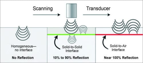

Fig. 1: Ultrasound launched into a sample is reflected not at all by a homogeneous material (left), moderately by interfaces between solids (centre) and almost completely by a solid-to-air interface (right)
There are tools available that use an ultrasonic transducer to scan back and forth just above the plastic-encapsulated IC, IGBT module or other sample. The transducer is coupled to the top surface of the sample by a column of water that travels with the transducer; ultrasound at such high frequencies does not travel through the air. While moving, the transducer passes over several thousand x-y locations each second. At each location the transducer launches a pulse of ultrasound, and records the echoes sent back by material interfaces at various depths within the sample.
Ultrasound pulsed into the sample is reflected only by material interfaces. Gates are set by the operator to define the depth range from which echoes will be accepted for imaging. Put a block of homogeneous silicon onto the stage with a gate that includes virtually all of the silicon but neither the top or bottom surface, and the sample will send back no return echo signals at all, as seen at the left of Fig. 1, and the acoustic image will be solid black. If the pulse has been set to have somewhat wider gate that includes both the top and bottom surfaces (interfaces) of the silicon block, these two interfaces will be imaged. In either case, some of the ultrasound will be absorbed and scattered as it passes through the silicon.
The amplitude of any return echo signal depends on the properties of the two materials at a given interface. The amplitude of an echo from the interface between two solids can range from just above a small percentage of the pulse to above 90 per cent, as seen in the centre of Fig. 1. But the amplitude of a return echo from any solid-to-air interface is invariably very nearly 100 per cent, as seen at right in Fig. 1. Even if the gap containing the air or another gas is as thin as a small fraction of a micron, the amplitude will be the same.
The time of flight of the return echo signals can also be recorded and used to measure the distance from a reference point to the interface from which the pulse is being reflected at a given x-y coordinate. In this way a buried contour such as a warped layer can be measured and imaged.
Fig. 2 shows the acoustic image of bonding of a heat-sink. The transducer scanned the area of the heat-sink and collected return echo signals from the gate depth, which encompassed the solder layer bonding the heat-sink to its substrate as well as the two interfaces (solder to heat-sink, and solder to substrate). Gray regions in the acoustic image represent partial reflection of the ultrasonic pulse from one or both of these interfaces.
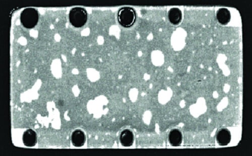
Fig. 2: White regions are air-filled heat-blocking voids in the adhesive material for this heat-sink
Black spots are images of holes for bolts that will hold the heat-sink in place. These are black because they run completely through the gated depth—that is, there is no interface within the gated depth to reflect ultrasound.
The irregularly shaped white features are voids within the solder. These were formed by air bubbles trapped in the fluid solder. The voids block heat flowing from the die, as do the intended voids around the bolts. The solid-to-air interface at the face of the void nearest to the transducer reflects virtually all of the ultrasound, and thus appears white in the acoustic image. At three of the four corners of the heat-sink, what appears to be an intended void surrounds the bolt; solder flowed into the void at upper left. There are smaller intended voids that partly surround most of the other bolts.
An engineer examining this image would find plenty of information to use in process control.
In Fig. 3, on the left is the optical image of a heat-sink bolted to the back side of a printed circuit board, where it dissipates heat from a component on the top side of the board. The acoustic image of the same heat-sink is shown on the right.
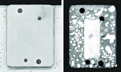
Fig. 3: Optical (left) and acoustic (right) images of a heat-sink on the back of a printed circuit board
The return echoes were gated on a depth from just above to just below the solder layer. The bolts are therefore black, similar to the bolts in Fig. 2. At the centre is the acoustic image of the cavity on the far side that holds the component. The numerous irregular white features are voids—air trapped in the fluid solder when the heat-sink was put in place. X-ray tends to miss thin features such as these because so little of the solid material is absent.
Practically, any heat-sink that is joined to its substrate by solder or another adhesive is subject to voids, non-bonds and other gaps that block heat flow from the die. In addition to imaging the adhesive layer, an acoustic microscope can measure and report the percentage of the bond area that is occupied by gaps.
IGBT modules are more likely to be imaged than many other items because their high power levels and the types of applications (subway cars and mine drilling equipment, for example) make the presence of gaps that can impede heat flow more critical. An inverted acoustic micro imaging tool meets the requirement of imaging IGBT modules through the heat-sink. Its transducer faces up to pulse ultrasound into the module and can create images at any depth, including the die attach near the top of the module.
Besides internal gaps, there is another reason to image IGBT modules acoustically: The heat-sink is bonded to a ceramic raft, which tends to warp or tilt. Even if there are no voids in the adhesive, a distorted raft makes heat flow from the die non-uniformly, and creates mechanical stresses within the die that can lead to fracture and electrical failure of the die.
Both anomalies—voids and raft distortion—are imaged by the acoustic microscope tool in a single scan of the module by using the Time Difference mode. The return echoes in this case do not report the amplitude of the echo. Instead, these report the distance of the reflecting surface from a reference point. The gate defining the depth range from which echoes will be accepted extends from just below the interface between the solder and the heat-sink to a depth just below the deepest point on the surface of the ceramic raft. The gate itself is planar, so the thousands or millions of echoes collected from x-y coordinates will create a surface contour map of the raft.
Fig. 4 shows the Time Difference image of one of nine ceramic rafts in an IGBT module. The colour spectrum maps the surface of the warped ceramic raft: the deepest points (nearest to the die) are yellow. Red, pink and subsequent colours are closer to the heat-sink. The black regions in the lower left and right corners are either in contact with the heat-sink or very close to it—that is, these regions are above the gate and imaged as black acoustic shadows.
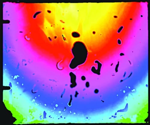
Fig. 4: Colours indicating specific depths map the warpage in the ceramic raft of an IGBT module. Black items (and smaller coloured items) are voids in the solder
Numerous voids of various sizes are also present in the solder. The black ones are above the gate and adjacent to the heat-sink; others are at the depth defined by their colour.
The die attach material above the raft in an IGBT module is a second location where voids may occur, and the acoustic microscope tool scanning the heat-sink can also image the die attach. The return echoes from the die attach must pass through the solder layer, with the result that voids in the solder (like those in Fig. 4) may hide some of the voids in the die attach. But an IGBT module with voids at both locations is likely to be rejected anyhow, although it can be reworked if not yet encapsulated.
Acoustic microscope tools have numerous other imaging modes that are useful in examining heat-sinks—non-destructive cross-sectioning, for example, or the ability to simultaneously make dozens of very thinly gated images at specific depths. In all cases, the goal is to image and analyse features that might interfere with heat flow.
