


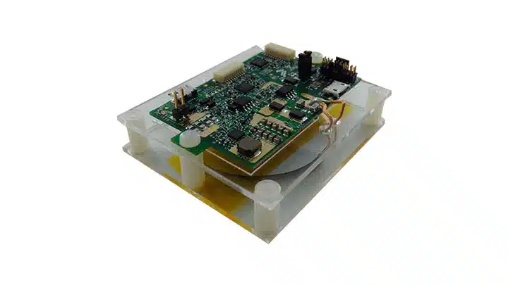
The compact 15 Watt wireless charging receiver design adheres to the Wireless Power Consortium (WPC) specifications and offers space-efficient integration.
Wireless charging enables convenient and cable-free power transfer to devices. It uses electromagnetic fields to transfer energy between a charging pad and a compatible device, eliminating the need for physical connections. This technology is increasingly integrated into smartphones, smartwatches, and other portable devices, simplifying the charging process for users. To simplify the design process, the NXP has launched the reference design for 15 Watt Buck Wireless Charging Receiver that supports larger form factors like the latest smartphones and tablets, catering to their need for faster charging. The design complies with the Wireless Power Consortium (WPC) and Medium Power Working Group (MPWG) specifications and can support forthcoming standards.
The receiver coil of the design receives input power ranging from 3.5 V to 20 V AC at its peak from the transmitter. It efficiently converts this input into an output power of 15 W, providing 5 V at 3 A. The design also supports Frequency-shift keying (FSK) communication signals from medium power transmitters. To ensure the safety and integrity of the system, the design incorporates hardware protection mechanisms for rectifier voltage, output voltage, and output current. It offers space-efficient integration with a compact Printed Circuit Board (PCB) size of 40 mm × 40 mm.

The reference design is based on the ARM Cortex M0+ processor with Ultrahigh Voltage (UHV) technology. The rectifier in this design utilizes a self-driven sync type and has an input voltage range from 3.5 V to 20 V AC at its peak, while the output voltage range from 3.5 V to 20 V DC. In terms of communication, the design incorporates Amplitude-shift keying (ASK) differential bi-phase signal modulation by switching the modulation capacitor. The FSK signal is also demodulated using the Computerised Numerical Control (CNC) and FSK demodulation timer (FSKDT) modules. For enhanced versatility, the CNC module detects input voltage from wired power plugs and automatically switches to wired power when the voltage falls within the 4.5 V to 5.5 V range. Moreover, the design features a DC-DC converter that accepts input voltage ranging from 5 V to 21 V DC, providing an output of 5 V DC with a current capacity of 3 A.
The design offers flexibility to accommodate various output voltages, catering to different application charging voltage requirements. The reference design incorporates interfaces such as a 12-bit analog-to-digital converter (ADC) and Programmable Gain Amplifier (PGA) for efficient power loss detection at the system level, ensuring Foreign Object Detection (FOD). The Inter-Integrated Circuit (I2C) and universal asynchronous receiver transmitter (UART) interfaces allow for secure communication between the receiver and the main application processor (AP), facilitating security measures or content delivery.
NXP has tested this reference design. It comes with a Bill of Material (BOM), schematics, etc. You can find additional data about the reference design on the company’s website. To read more about this reference design, click here.
