The wireless charger solution utilizes a low-cost microcontroller and enables charging through resonant inductive coupling facilitating efficient power transfer between transmitter and receiver.
Wireless charging, also known as inductive charging, is an innovative technology that enables the transfer of electrical energy between two coils through electromagnetic induction. Recently, it has gained significant popularity and become a prominent feature in various mobile devices, including smartphones. Renesas have launched a reference design for the wireless charger to simplify the design process. The reference design features advanced functionalities, such as overcurrent monitoring, that use the robust analog capabilities of the used microcontroller unit (MCU). The system comprises a charging pad and a compatible device positioned on top of the pad. Charging occurs through resonant inductive coupling, enabling efficient power transfer between the two components.
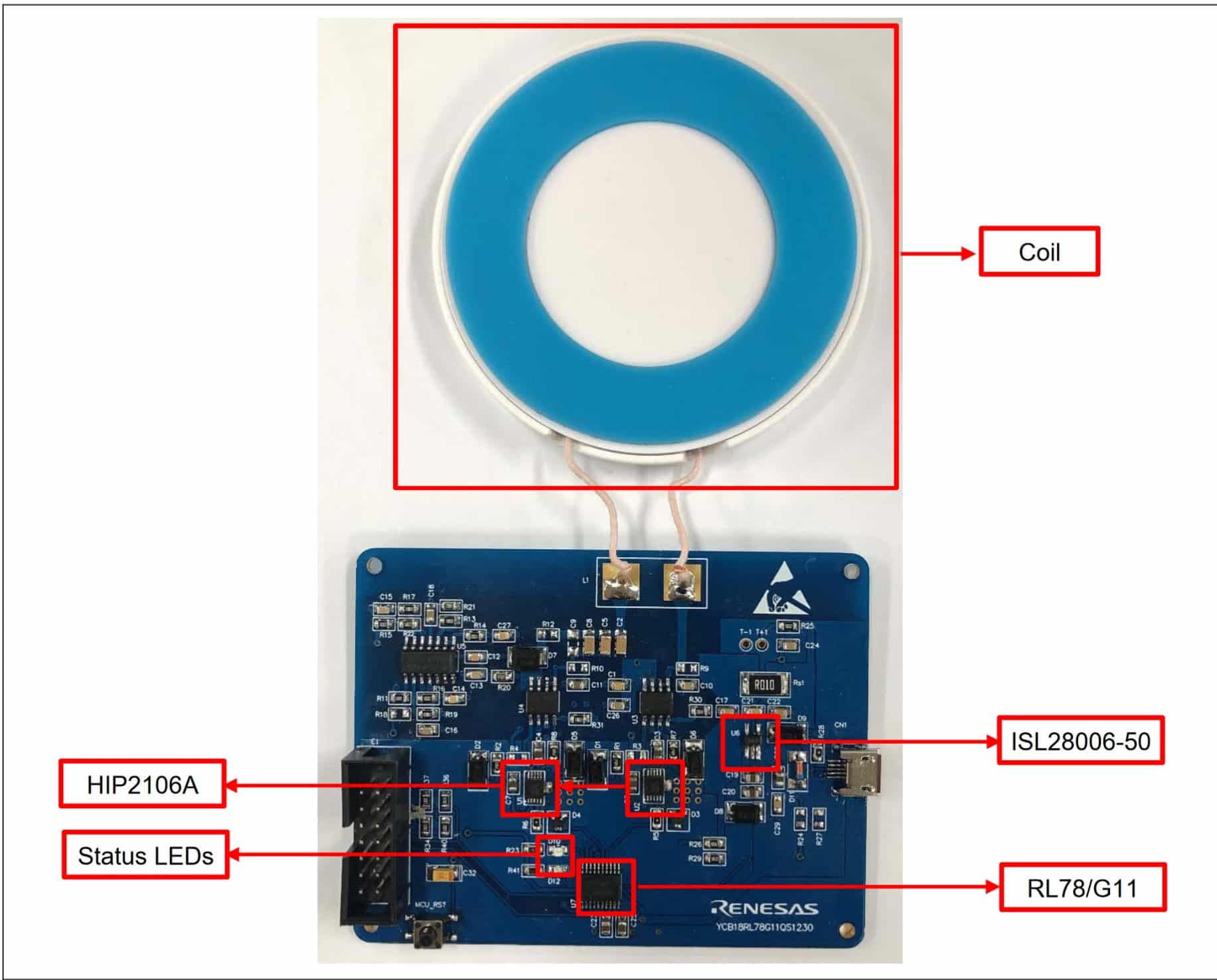
The reference design features Qi, an open interface standard as a wireless charging standard. The design operates at a Direct current (DC) power supply of 5V. The system’s operating temperature ranges from -10°C ~ 45°C, and operating humidity ranges from 5 ~ 99% RH. The maximum charging current provided by the wireless charger is 800mA, and the maximum output power is 4 watts. The reference design specification includes a visual indication function as some LEDs are used to indicate various information such as detection of a receiver, over current, over temperature, etc. The design of this system relies on the RL78/G11 Microcontroller as its core component. Various peripherals of the microcontroller, including analog-to-digital converters, Programmable Gain Amplifier (PGA), 16-bit timer, timer array unit channel 3, and input-output ports, are strategically utilized to address specific use cases within the system.

The wireless charging transmitter is composed of various components, including a DC 5V power input, a current sense amplifier, a voltage detection circuit, a temperature monitor circuit, a main MCU, an LED indication circuit, a Pulse Width Modulation (PWM) driver circuit, and a coil. Due to the relatively high consumption current of the wireless charging transmitter, the design requires an external DC 5V power adapter to provide the necessary power supply. The micropower current sense amplifier ensures efficient operation with its wide input voltage range and low power consumption. If the power supply voltage falls outside the acceptable range of 4.5V to 5.5V, the power transmission process will not commence. For this purpose, a voltage detection circuit is included in the design. When the temperature of the transmitter coil continuously measured using a temperature monitoring circuit exceeds the established safety threshold of 60°C, the power transmission will be automatically halted.
Renesas have tested this reference design. It comes with a Bill of Material (BOM), schematics, Printed circuit board (PCB) layout, etc. You can find additional data about the reference design on the company’s website. To read more about this reference design, click here.