
The basic requirements for power semiconductors are efficiency, reliability, controllability, and cost-effectiveness. Breakthroughs in wide-bandgap semiconductors, especially in gallium nitride (GaN), have enabled devices with high conductivity and hyper-fast switching, with a silicon-like cost structure and fundamental operating mechanism. This article discusses some design aspects for implementing GaN transistors in power converters.
With emerging technologies like electric vehicles, there is a need for power converters that are highly efficient and have high power density. Silicon devices based power converters are limited in terms of efficiency and power density, as silicon MOSFETs cannot switch faster than around 500kHz frequency. Thus arises the need for wide bandgap semiconductors that feature high voltage operation, high current handling capacity, are low on resistance, have lower switching loss, and high frequency operation.
Silicon carbide and gallium nitride are two most popular wide bandgap materials. Gallium nitride or GaN transistors are currently widely used for applications ranging from electric vehicles to phone chargers. High power density of GaN devices allows compact power circuits and fast power delivery.

What makes these GaN devices special is their low ‘on’ resistance and very low gate capacitance. The low on resistance and low gate-drive capacitance makes it possible for GaN devices to switch hundreds of volts in nanoseconds, giving it multiple megahertz capability. This capability leads to smaller power converters and higher fidelity class D amplifiers.
The switching frequency is also limited by the series gate resistance of the transistor. The gate resistance limits how quickly the capacitance of a field effect transistor can be charged or discharged. The metal gates enable GaN to have gate resistances of a couple of tenths of an ohm. This low gate resistance also helps with dV/dt immunity.

However, two major problems are common in the application of wide-bandgap devices: voltage overshoots and oscillations. Wide-bandgap semiconductor devices operate at much higher frequencies than silicon based devices. The faster switching speed means higher dv/dt (change in voltage with respect to time) and di/dt (change in current with respect to time), which leads to greater oscillation challenge.
Various kinds of oscillations arise under different circumstances, but one of the prominent kinds is sustained oscillation of the drain-source voltage. This problem occurs only in GaN transistors as they do not incorporate body diodes. When the gate-source voltage or the gate-drain voltage is higher than the threshold voltage of the GaN device, the electrons are attracted to the heterostructure interface of the aluminium gallium nitride (AlGaN), and GaN devices conduct reverse current under such conditions. The sustained oscillation may occur due to the reverse conduction characteristics of GaN devices and parasitic parameters.
The switching oscillations can cause many undesired negative effects, including voltage and current overshoots, shoot-through, EMI, additional power loss, and even device damage, which can seriously affect the performance of power converters and systems. Voltage and current overshoots are common in GaN devices during turn-on and turn-off transients. For a device operating at 600V, the voltage overshoots can peak at 800-900V, resulting in a catastrophic failure.
In addition, high dv/dt and di/dt may cause the gate-source voltage to exceed the threshold voltage, thereby inducing false turn-on. When false turn-on occurs, the power loop inductance has an input voltage across it, and therefore a large short-circuit current will pass through the two switches. From various experimental results, the short-circuit current rises to nearly 150A, which seriously affects the performance and reliability of the system.
The high dv/dt and di/dt, moreover, cause severe conducted and radiated EMI noise. Conducted and radiated EMI emissions often produce undesirable effects on electronic systems such as radio receivers, medical equipment, and communication systems. Besides, they cause malfunctions and non-operations in control systems.
Apart from degradation in performance, the oscillations in GaN circuits can also cause additional power loss. There are various conventional and unconventional ways, apart from active gate drivers, to suppress these issues occurring due to high dv/dt and di/dt.
Following are some of the design and PCB layout tips to reduce these effects and their impact on the overall device performance.
Design tips for gate driving
1. Switching speed control
Switching speed is limited by the low-pass filter formed at the gate due to the gate resistance and gate capacitances. One can easily control the switching speed by adding an external gate resistor. The external gate resistor will increase the time constant associated with the pole and decrease the maximum switching speed. On the other hand, it will play a crucial role in limiting noise and ringing in the gate drive path. It is observed that the parasitic inductances and capacitances, high dV/dt and di/dt, and body-diode reverse recovery can cause unwanted behaviour without an appropriately sized gate resistor.

Fig. 1 depicts the common gate elements in the gate drive path: the internal resistance of the gate driver, external gate resistance, and internal gate resistance of the MOSFET or IGBT. It can be easily observed that the external gate resistance is the only component that tunes the gate drive waveform.
It is very important to select an optimum gate resistor for a high-performance design. Following points should be considered while selecting an external gate drive resistor:
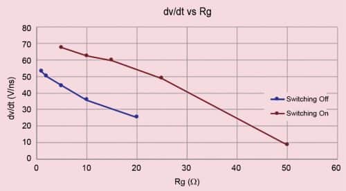
- The switching characteristics of both turn-on and turn-off are dependent on value of the gate resistance. The greater the gate resistance, the longer the switching time and the greater the switching loss. Also, as the gate resistance increases, the surge voltage during switching becomes smaller. So, there is a trade-off between switching speed and overshoots.
- The greater the RG, the more unlikely a dv/dt shoot-through current becomes.
- Various switching characteristics are varied for stray inductance. Therefore, the gate resistance needs to be designed on the lower stray inductance condition.
All the above points suggest that the value of gate resistance must be maximised in order to suppress overshoots, and all other problems induced by high dV/dt and di/dt. But increasing the resistance will lower the switching speed. Therefore, an optimal value is crucial.
It is recommended to select the gate resistor that will give your design a quality factor Q between 0.5 and 1. A quality factor greater than 0.5 offers faster turn-on and turn-off when required.
For selecting an optimal value, record the gate drive ring with no external resistor. This is the ring frequency ƒR. Plug this value in the following equation to calculate the source inductance LS. The value of Ciss can be found in the device datasheet.
LS=1/(CISS(2πƒR)
Determine the gate resistance from this equation, where RG is the gate resistance:
Q = ωLS/RG
You can also select the optimal value by simulating, starting from 0 ohms of external resistance. Fig. 3 show the impact of external gate resistance on overshoots.

The trade-off between fast rise and fall times vs overshoots and oscillations is why the external gate resistor element of the gate-drive design is so valuable.
2. Implementing negative drive voltage
Negative drive voltage is not required, but it is often beneficial. In many cases, negative drive voltage can increase noise immunity and reduce switching loss.
While driving high-power GaN systems, there is a risk of Miller effect induced turn-on when a high rate of change of voltage (high dV/dt) is seen across the power device. In such scenarios, current is injected onto the gate of a power device through the gate-to-drain or gate-to-collector capacitance. The parasitic turn-on results in lower efficiency or even device failure.
The Miller effect can be alleviated by creating a low impedance path from the power device gate to the source or drain, by increasing the gate resistance, or by driving the gate to a negative voltage with respect to the source or drain. Here, we will discuss the latter option.
The goal is to keep the gate voltage below a desired threshold when a current spike through the Miller capacitance occurs.
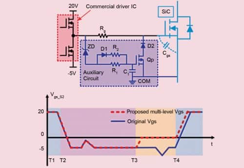
For implementing negative drive voltage there is no need to look for gate drivers supporting negative gate drive voltage. One of the common methods is to offset the gate driver from the power device, thereby creating a negative gate drive relative to the source or drain of the power device, while the gate driver IC still sees a unipolar supply only.
The isolated gate driver ICs, however, feature under-voltage lockout (UVLO) to prevent a power device from being driven weakly if the gate driver is being driven with too low of a gate voltage. Two separate voltage sources can be created to tackle this issue. But the trade-off here is with cost.
“Many existing gate drivers that are unipolar in operation can be operated to easily drive a gate negative with minimal external circuitry. There are some implications to consider such as the effective UVLO voltage, but the benefit of such operation is great,” says Ryan Schnell, Applications Engineer at Analog Devices.
Moreover, there are certain types of devices that require a negative voltage to be fully off, necessitating some kind of negative voltage drive coming from the gate driver. Fig. 4 shows the influence of negative drive voltage on switching loss.

3. Controlling switching speed to avoid unexpected turn-on
As discussed, there are three ways to avoid the problem of Miller effect. First, by creating a low impedance path from the power device gate to the source or drain. Second, by increasing the gate resistance. Third, by driving the gate to a negative voltage with respect to the source or drain.
To create a low impedance path from the gate to source, we can add a capacitor (gate-source capacitor). The addition of capacitance produces the same effect as increasing the gate resistance. Both of these will limit the maximum switching frequency by reducing the dV/dt.
To avoid unexpected turn-on, recommended gate-source capacitance is two times value on the specification sheet.
4. Managing dead time loss
Dead time loss occurs in an FET when the current flows from the source to drain while the FET is turned off. In silicon FETs, a body diode is present which typically turns on at about 0.7V. GaN HEMTs do not have a P-type material, hence the body diode is absent.
The conduction from drain to source happens when the drain drops below the gate by more than the threshold voltage of the device. When this happens, the FET turns on backwards with the gate-to-drain voltage turning on the device. The drain falls much below the threshold voltage of the transistor when the FET is on, which effectively appears as voltage drop plus a drop proportional to 1/transconductance.
In power converters, there is a short time in each cycle—the dead time—where neither switch is on, and the inductor current is forced to flow through one of the FETs. The energy lost in the dead time is proportional to the current, voltage, and the amount of time spent in this mode, which corresponds directly to the dead time.
It can be easily deduced that the dead time must be minimised for low power loss. But smaller dead time will result in the loss of zero voltage switching. If the dead time goes negative, however, cross conduction will occur with the associated loss in efficiency.
Therefore, the dead time must be held to a small band without straying outside it.
Smaller dead time and negative voltage driving can increase the efficiency of the power converters significantly. Nowadays, gate drivers come with programmable dead time. When determining what dead time is sufficient for a circuit, various mismatches and effects of propagation delay must be taken into consideration for precise control. Following are those aspects:
- Mismatch of the driver. For drivers with separate high and low side inputs, it is important to look for the difference in propagation delays
- Propagation delay variation with high-side ground
- Variation with bootstrap voltage
- When the signal is propagating through the level shifter simultaneously with a switching transition
5. Crosstalk suppression
When GaN devices work at high frequencies, the high dv/dt and di/dt due to parasitic inductances and capacitances leads to oscillations and overshoots in gate-source voltage and affect the stability of driving circuits. Moreover, it gives rise to crosstalk between the upper and lower switch in certain topologies.
The circuit in Fig. 5 can effectively suppress crosstalk as it can maintain an appropriate negative voltage when the gate positive voltage peak occurs and pulls up the gate voltage to a less negative voltage level or zero level before the gate negative overshoot event occurs. This circuit raises the gate voltage to 0V and clamps it at 0V after the false triggering period, and before the turn-on signal arrives. This makes the negative gate overshoot occur at 0V level, reducing the risk of negative breakdown. Moreover, a low turn-off impedance path is created to suppress crosstalk, which can limit the positive and negative false triggering voltage peaks to the required range because the common source inductor (CSI) is decoupled and displacement current of the gate-drain capacitor is bypassed.
6. Adding ferrite beads or RC snubbers
Ferrite beads are well known for suppressing high-frequency electronic noise in electronic circuits. They employ high-frequency current dissipation in a ferrite ceramic to build high-frequency noise suppression devices. It is a common method of inserting ferrite beads into the power loop to dampen parasitic ringing.
The equivalent circuit of the ferrite bead is a series connection of frequency-dependent resistor and inductor. Therefore, the ferrite bead and the device parasitic capacitance form a second-order circuit with oscillation frequency expressed as ƒOSC = 1/2π√CeqLeq.

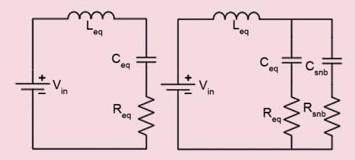
Here, Ceq is the equivalent parasitic capacitance of the device, and Leq is the equivalent parasitic inductance of the circuit and the ferrite bead.
The damping coefficient is given by:
m = Req /2√Leq /Ceq
where Req is the resistive part of the impedance of the ferrite bead.
For suppressing the parasitic ringing effectively, following conditions must be satisfied:
- The damping coefficient m must be greater than 1
- The above condition needs to be met at the oscillation frequency, and the ferrite bead impedance at the oscillation frequency should be mainly resistive
- The DC power loss of the ferrite bead should be low
Talking about RC snubbers, they are a combination of impedances used to suppress the rapid rise in voltage across a switching device. The voltage across a parasitic capacitor cannot change instantaneously, so a decreasing transient current will flow through it for a fraction of a second, allowing the voltage across the switch to increase more slowly when the switch is opened.
At the gate of the GaN transistor, second-order RLC model can be used for parasitic ringing during the turn-on and turn-off transients of the device. RC snubbers can be designed to suppress this parasitic ringing. The snubber elements can be valued as follows:
Rsnb (s) = (1/2ζ)(√Lp /Cp )
Csnb(s) = 1/2πRsnb ƒr
where ζ is the damping ratio, Lp is the parasitic capacitance, Cp is the parasitic capacitance of the device, and ƒr is the oscillation frequency.
PCB layout practices
Parasitic inductances and capacitances are introduced by device packaging and PCB layout. By optimising the PCB layout, we can suppress the effects of parasitic elements and as a result reduce oscillations and ringing. PCB layout techniques can minimise the power and drive loop inductance, and the optimal double-sided layout can reduce the power loop inductance significantly, suppressing the oscillations effectively.
Reducing parasitics via PCB layout has the benefit that it does not require any additional auxiliary circuit. But with this, the layout may become complex, and these techniques are rather hard to implement.
Impact of PCB layout parasitics
To intuitively understand how each major parasitic element in PCB layout affects the performance of the circuit design, we model the circuit with device and parasitic inductances and capacitances.
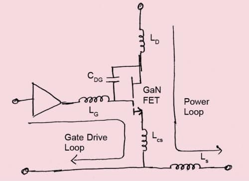
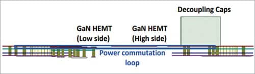
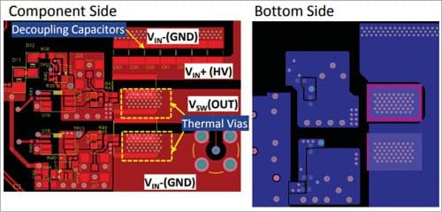
The power loop inductance (LD/LS) is one of the major parasitic inductances affecting the reliability of the system. Due to this inductance, overshoots and ringing occurs during turn-on and turn-off transients. To reduce these effects, the power loop length must be minimised and the decoupling capacitors must be placed close to the power device.
Another major inductance is common-source inductance (LCS) or CSI. This inductance slows down the switching speed and gives rise to gate ringing and oscillations. It is critical from a stability viewpoint. For minimising the effect of this parasitic inductance, Kelvin connection must be implemented to source.
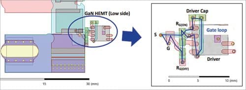
From the driver and gate interface, we get gate-loop inductance which causes undershoots, overshoots, and false turn-on. For suppressing its effects, the gate driver must be placed close to the GaN FET to minimise gate loop.
Talking about parasitic capacitance, gate-drain coupling capacitance is by far the major parasitic capacitor. This capacitor limits the switching speed and participates in sustained oscillations. To minimise its effect, overlapping between drain and gate drive copper pour or track must be avoided.
Recommended practices
Following are some of the recommended PCB layout practices summarised for optimal performance:
- Place the gate driver close to the GaN FET and minimise the gate drive loop area and length for optimising gate drive loop
- Increase RG or use a ferrite bead on the gate if gate oscillation is observed
- Use a tight layout to minimise power loop length and place the decoupling capacitor as close as possible
- Minimise noise coupling due to PCB parasitic capacitance
- Minimise overlapping between drain side power connection and gate drive signal track
- Design for low thermal resistance using thermal vias and copper pours
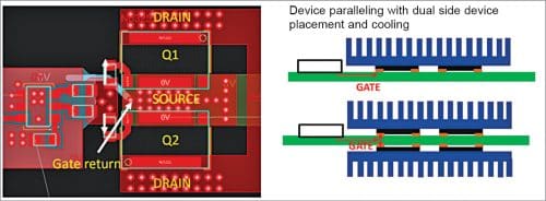
- When paralleling, implement dual side placement with optimum layout. Use individual gate resistors and star connection for gate drive.
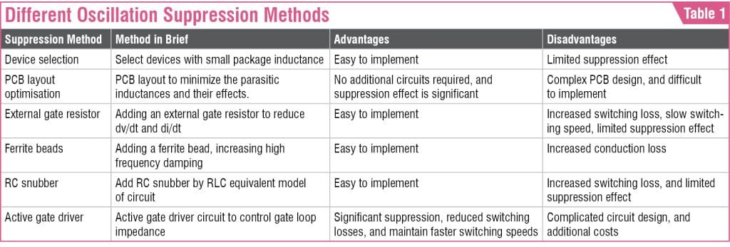
In this article, we came across various oscillation and overshoot suppression techniques. Table 1 shows comparison among them.