The importance of via holes cannot be ignored by the designers of multi-layered PCBs. This article describes various types of via holes and how they help in proper designing of the PCBs.
It is a well-known fact that a PCB is the heart of an electronic system. Hardware engineers have lots of expectations from PCB designers with respect to signal integrity, power integrity, electromagnetic compatibility (EMC) as well as thermal analysis. Depending upon the type of circuit, all these parameters need to be managed in a PCB design so as to make an assembly successful for its intended use.

In this digital world the signal speed ranges from a few MHz to several GHz. With the increased demand of functions per assembly/chip and miniaturisation of electronic systems, PCBs are becoming more and more complex. The increasing requirement of multiple functions in a chip is resulting in complex surface mounted device (SMD) components, which have multiple pins placed close together or are even leadless packages. The multi-pin components like ball grid arrays (BGAs) and thin quad flat packages (TQFPs) force the PCB designers to go for multilayer PCBs.
Via holes play a major role while designing the multilayer PCBs. A via hole is a plated through hole (PTH), which is used to transfer a signal from one layer of a PCB to another layer, without the scope of mounting any component into these holes.
Most engineers make use of via holes just to transfer signals. But there are other features too that are associated with these via holes. These via holes can be used in various ways. A via hole can have a positive impact when it comes to route a signal (interconnection) and a negative impact when it comes to route a sensitive signal.

Various type of via holes
Through hole via, where one can see through a PCB. Such a via hole starts from the top layer of a PCB and ends at the bottom layer. It must be defined in each and every electrical layer of a PCB.
Blind via, whose starting point is visible, but end point is not visible. Such via holes are used in multilayer PCBs. A blind via starts from an outer layer and disappears in inner layers.
Buried via, which is not visible at all. It is used to transfer a signal from one inner layer to another inner layer. A buried via is used to save the space for signal routing over outer or inner layers.
Micro via, which has a comparatively much smaller drill diameter. Due to shrinkage of electronic assemblies and routing of high-density-interconnection PCBs, via size (diameter) is getting reduced. As per IPC, any via hole having drill diameter of less than or equal to 0.15mm is a micro via. Such via holes are laser drilled.
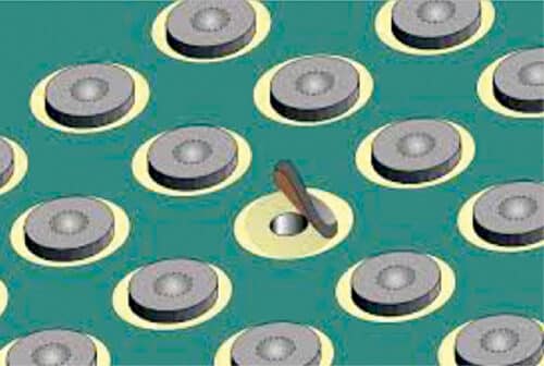
Via-in pad is generally used where it becomes difficult to put a via hole in between the pads/land area due to limitation of available space. In this case, a via hole is drilled inside a land area, and we can say that the land area is converted into a pad. Such via-hole’s diameter must be small (as per manufacturer limitations) as there may a chance of solder theft at the time of reflow soldering. Components like bill grid array (BGA) require via-in pads. (Land area is a copper area without a hole, where an SMD component is soldered. A pad is a copper area with a hole in the centre.)
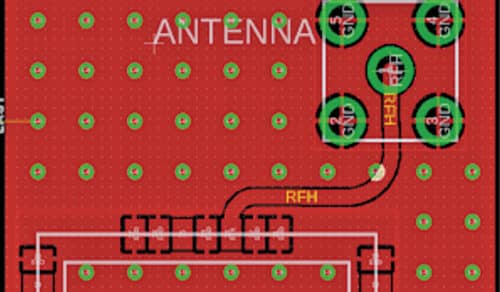
Via for stitching is also used to interconnect large copper areas on different layers. It helps reduce the return path of signals and thereby maintain low impedance. A via shielding is created by placing one or more rows of via holes along the signal route path, which helps in reducing electromagnetic interference (EMI) and crosstalk.
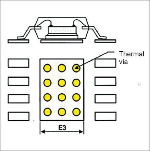
Thermal via is used to improve the heat dissipation of surface-mount components rather than transferring a signal. Structurally, a penetrating hole is opened in the board. Thermal resistance depends on the area and thickness of the copper foil on the PCB that serves to dissipate heat, as well as on the thickness and material of the board.
In order to effectively use thermal vias, it is important that the thermal vias be located close to heating elements, such as directly below the components. As indicated in Fig. 4, the effect of thermal equilibrium is utilised, and so it should be apparent that connecting areas with large temperature differences is a good plan.
Via holes and signal integrity
In case of low frequency, vias do not affect signal transmission. As frequency rises (above 1GHz) and signal rising edge becomes steep (1ns at most), however, vias cannot be simply regarded as a function of electrical connection, and influence of vias on signal integrity has also to be considered. Vias behave as breakpoints with discontinuous impedance on transmission line, causing signal reflections.
Nevertheless, issues brought by vias concentrate more on parasitic capacitance and parasitic inductance. The influence of via parasitic capacitance on a circuit is primarily to prolong the rising time of signals and reduce the running speed of circuit. Parasitic inductance, however, can weaken the contribution of bypass circuit and decrease filtering function of the whole power system.
The larger the via diameter is, the more discontinuity via will cause in high-frequency and high-speed PCB designs. It is tentative information, since it also depends upon position of power planes, via hole diameter, plating thickness, etc. It should be kept in mind that a single via is going to add 1-3nH of inductance in the signal. Further study is required if a designer comes across such a situation. This is known as Black Magic over a PCB when compared with circuit simulation results.
Current carrying capacity of a via
Generally, I never recommend switching a power rail between the layers when designing a power PCB. However, one can use component-mounting pads for the same. If it becomes necessary, then use multiple via holes.
As per researchers, calculating current carrying capacity of a via hole is a function of multiple factors like, length of via, its drill diameter, placement of power planes, amount of power to be switched between the layers, glass transition temperature (Tg) of PCB base material, copper plating thickness, etc. As a thumb rule the finished diameter of a via hole must be at least as large as the trace width divided by three. For a digital circuit, the use of via holes for VCC or Ground is obvious since the amount of power is very less.
Planning via holes diameter for your design is of great concern with respect to a manufacturer’s capabilities. You may plan different via hole diameter for a PCB as per your requirement.
Most common drill diameter of a via hole is 0.5mm (20mils), which can be drilled by most PCB manufacturers. If you are planning anything less than this, you must check the manufacturer’s drilling and plating capabilities.
With the reduction in drill diameter, the spindle speed of a CNC PCB drilling machine needs to be high. That’s why micro vias are laser drilled instead of mechanical drilling.
Shavinder Singla (CID-IPC, USA), Senior Technical Officer, Centre for Development of Advanced Computing, Mohali (Punjab)