
Electromagnetic interference can derail your PCB’s performance. EMI management is not just a technical necessity but a hallmark of exceptional PCB design.
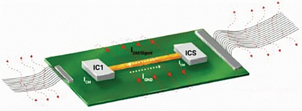
Electromagnetic interference (EMI) poses a critical challenge in printed circuit board (PCB) design. It occurs when electrical signals produce unwanted interactions through magnetic fields, potentially disrupting electronic circuit performance.
Managing EMI is a core responsibility for PCB designers, who must ensure that designs comply with regulatory noise limits.

To meet global EMI standards, PCBs undergo extensive testing, including radiated immunity, conducted emissions and immunity, electrostatic discharge (ESD), electromagnetic fields (EMF), and surge immunity. These tests are expensive, so designers must identify EMI issues before testing.
Table of Contents
Relationship Between Electric Signals and Magnetic Fields
Maxwell’s equations encapsulate the fundamental relationship between electric signals and magnetic fields, which describe how varying electric fields can generate magnetic fields and vice versa.
When current flows through a conductor, it generates a magnetic field around it. High-frequency signals or large current spikes can produce strong electromagnetic fields that may interfere with nearby electronic components, leading to EMI.
PCB Stack-up and Layer Configuration
A well-planned PCB stack-up can significantly reduce EMI. A typical multilayer PCB consists of signal layers, power planes, and ground planes. Proper placement and configuration of these layers are critical.
Signal layers. High-speed signal traces should be routed on internal layers sandwiched between ground planes. This arrangement helps contain the electromagnetic fields within the PCB and reduces radiated EMI.
Power and ground layers. Power planes should be placed adjacent to ground planes to create low-inductance paths for return currents. This configuration also provides good decoupling and reduces noise.

Trace routing. Keep high-speed traces short and direct. Use differential pairs for high-speed signals to minimise EMI by cancelling out magnetic fields generated by each trace.
Also Check: High-Speed PCB Design Guide
Partitioning PCB into Digital and Analogue Sections