


High-speed PCB design consists of multiple steps. Design re-spin is not only cost-sensitive but also time-consuming. So, one should follow proper design rules early in the design cycle to have the PCB working at the very first attempt
Printed circuit board (PCB) is an essential part of all electronic goods, starting from electronic toys, remote controls, and mobile phones to complex electronic circuits in telecom equipment, airplanes, spacecraft, and medical devices. With rapid advancements in the electronics industry and the miniaturization of components, PCB design has gone through a rapid evolution in the last few decades.
From PCBs of a few layers and mostly through-hole components, PCBs nowadays have tens of layers, fine-pitch components, and a mixture of through-hole and surface mount components. Modern complex designs at times require flexible PCBs and embedded components.
PCBs that are designed for high-speed signals (more than 1Gbps) need special attention during design as signal quality (rise/fall time, crosstalk, attenuation, etc) plays a crucial role in reliable operation. High-speed PCB design consists of multiple steps. Design re-spin is not only cost-sensitive but also time-consuming.
High-speed PCB Design Flow
It is better to follow proper design rules early in the design cycle to have the PCB working at the very first attempt. Fig. 1 shows the major steps involved in a high-speed PCB design. Let’s go through the major steps one by one.

Schematic design: The design starts with a schematic drawing. There are many open sources as well as licensed software available for schematic design. But while designing a complex PCB design, it is better to go for reputed licensed versions as they offer better integration with the layout, useful features for quicker designs, and better constraint management.
During schematic drawing, the focus should be on the functionality of the circuit and the selection of components. During the selection of the components, the specifications to look for are size, power handling capacity, footprint, stray inductances and capacitances associated with that component, operating temperature range, and moisture sensitivity level (MSL).
Although the systems on chips (SoCs), field programmable gate arrays (FPGAs), and application-specific integrated circuits (ASICs) mostly come in ball grid array (BGA) packages, some ICs are available in multiple packages like SSOP, TSSOP, SO, etc. The key considerations to select a package are cost, temperature range, heat dissipation, real estate on the PCB, and lead time.
After the parts are finalized, symbols and footprints corresponding to those parts need to be created to proceed with the schematic. It is important to review the design carefully to check the desired functionality and any mistakes like wrong connection, unconnected nets, incorrect package selection, etc.
Component footprints also need to be checked carefully for their mechanical dimensions, pin sequences, etc. Only after that the final netlist and the bill of material (BoM) should be generated.
PCB stack-up and board mechanical: The PCB stack-up decides which layer would be used for signal routing and which ones for power and ground planes. The number of layers required for a particular design may be decided based on requirements, recommendations of the device datasheets, and the designer’s experience.
The board mechanical, or PCB template, is an auto-CAD drawing that specifies the shape and dimensions of the PCB, coordinates of the components sitting at the edge of the PCB (mostly connectors, LEDs, switches, jacks, etc), mounting holes, and other constraints that might be specific to the design.
The template may require minor modifications after the thermal simulation is done, as additional mounting holes may be required to fix heat sinks if required.
Thermal simulation: During the thermal simulation of the PCB, rough placement of the major heat-generating ICs, power supplies, components with special features (for example, a tall capacitor that might be blocking airflow), and ambient operating temperature need to be specified. Thermal inputs for an IC include total heat dissipation, maximum junction temperature, and thermal resistance parameters.
For pluggable modules in cages, the thermal model is required for accurate simulation. Thermal simulation may recommend modifying the placement if required. Also, the simulation decides the specification of fans, if required for cooling.
Placement and routing: One of the most critical and time-consuming steps in high-speed PCB design is component placement and routing. PCB layout is nothing but a multivariable optimization problem, the solution to which just gets better with experience. PCB layout includes defining constraints like keep-outs (where routing and/or planes are not allowed), placement of the components, routing of signals, creation of power and ground planes, optimization of routes, removal of unwanted vias, and cleaning of designs from extra traces or stubs.
In complex high-speed PCBs, signal integrity (SI) analysis (explained in the next step) is a crucial step. It is generally done in two phases—Pre-SI (before routing) and Post-SI (after routing). Also, we need to perform Design For Manufacturing (DFM) or Design For Assembly (DFA) checks to avoid any last-minute issues.
After the routing, its review, and SI analysis are done, the next step is back annotation where the components on the PCB are renumbered in sequential order based on their location on the PCB. This process helps in finding any component that may have been missed during debugging and board-level hardware testing.
SI analysis: SI (signal integrity) is a key challenge for the circuit to function properly. Many PCB design efforts fail just because signal integrity is not maintained.
SI is a set of measures of the quality of an electrical signal. Over short distances and at low bit rates, a simple conductor can transmit this with sufficient fidelity. At high bit rates and over longer distances, or through various mediums, various effects can degrade the electrical signal to the point where errors occur and the system or device fails.
In designs with high-speed interfaces like DDR3, DDR4, PCIe, etc, pre-layout SI simulations give a rough idea of whether the link will operate with fidelity after the actual layout. Change of positions of DDR and controller may be required to optimize the distance between the source and destination IC. Also, schematic modification may be required to incorporate additional termination circuits.
After the layout is complete, the post-layout SI simulation is performed for final confirmation incorporating all constraints.
Know your PCB Traces
Routing of signals on a PCB is generally done through two types of waveguide structures, namely microstrip, and stripline. Stripline is a transmission line trace surrounded by dielectric material suspended between two ground planes on internal layers of a PCB. Microstrip routing is a transmission line trace routed on an external layer of the board. Because of this, it is separated from a single ground plane by a dielectric material.
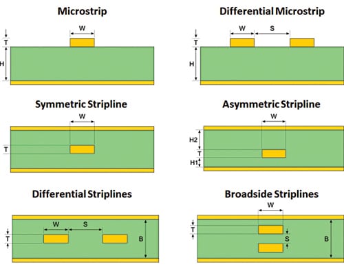
There are multiple variations of these two types of waveguides available, as shown in Fig. 2. Due to the complexity of the fabrication of PCBs, broadside and asymmetric strip lines are seldom used.
Vias
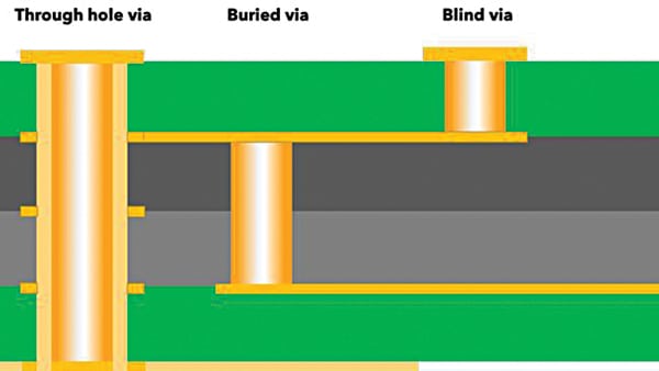
Via is vertical interconnect access. When a signal travels from one layer to another layer via is used. There are three types of vias in PCBs.
Through-hole vias are those that travel from the top layer to the bottom layer of the PCB. Blind vias are from either the top or bottom layer to an inner layer of the PCB. Buried vias are between two inner layers of the PCB with no access to them after the PCB manufacturing.
Through-hole vias are the most common. Buried and blind vias are costlier to manufacture. Fig. 3 shows different types of vias in a vertical cross-section of a PCB.
Choosing PCB Materials
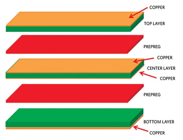
Due to manufacturability, high-speed PCB layer count is generally an even number. The basic components of PCB manufacturing are core and prepreg.
The core is a layer of dielectric with copper on either side. The layer of dielectric is formed between two smooth foils of copper, to a specified thickness. Prepreg, which is an abbreviation for pre-impregnated, is used by PCB manufacturers to glue together etched cores, or a copper foil to an etched core. Fig. 4 shows the construction details of a 4-layer PCB as an example.
The choice of PCB material depends on the application. FR4 (FR stands for Flame Retardant) material is the most used nowadays. However, very high-speed designs require other materials like Megtron6.
A few parameters that need to be kept in mind while checking various PCB materials for use are:
Dielectric constant (Dk): The dielectric constant (Dk) of a PCB material is generally between 3.5 and 5.5. A material’s Dk level will usually drop as the frequency rises. For a material to be safe for high-frequency applications, it must maintain a stable dielectric constant over the entire range of frequencies of operations.
The higher the relative dielectric constant, the slower a signal travels on a wire, the lower the impedance of a given trace geometry, and the larger the stray capacitance along a transmission line. Given a choice, the lower dielectric constant is preferable.
Loss tangent: A material’s loss tangent gives a measure of the power lost due to the material. The lower a material’s loss tangent, the better is the material.
The Tan δ of most PCB materials ranges from 0.02 for the most used materials to 0.001 for very-low-loss, high-end materials. It also varies with frequency, increasing as frequency increases. Loss tangent is usually a critical consideration at frequencies greater than 1GHz.
Glass transition temperature: Glass transition temperature (Tg) is the temperature range in which a PCB substrate transitions from a glassy, rigid state to a softened, deformable state as polymer chains become more mobile. When the material cools back down, its properties return to their original states.
Decomposition temperature: Decomposition temperature (Td) is the temperature at which a PCB material chemically decomposes (the material loses at least 5% of its mass). A material’s Td is an important ceiling when assembling PCBs, because when a material reaches or surpasses its Td, changes to its properties are not reversible.
Choose a material where you can work in a temperature range that’s higher than Tg but well below Td. Most solder temperatures during PCB assembly are in the 200ºC to 250ºC range and, luckily, most materials have a Td greater than 320ºC.
Coefficient of thermal expansion: The coefficient of thermal expansion (CTE) is the rate of expansion of a PCB material as it heats up. As a material’s temperature rises past Tg, the CTE will rise rapidly.
The CTE of a substrate is usually much higher than copper, which can cause interconnection issues as a PCB is heated. CTE along the X and Y axes are generally low—around 10 to 20 ppm/ºC. The CTE along the Z-axis should be as low as possible, and this will increase rapidly as a material surpasses Tg.
To reduce the higher expansion above Tg, choose a material with a higher Tg, at least 170ºC, and a low Z-axis CTE at a temperature greater than Tg.
Some Common Mistakes to Avoid During High-Speed PCB Design
- Use proper trace width as calculated from the layer stack-up for the required characteristics impedance.
- For power and ground traces and planes, the width must be sufficient to carry the current.
- Place decoupling capacitors near/below the power pins.
- Make separate grounds for analog and digital signals.
- Make sure the reference plane for critical signals is continuous end to end.
- Follow any special layout recommendations given by the IC manufacturer.
- Never route sensitive digital signals over high-voltage power planes.
- For differential signal length tuning, always match the asymmetric side.
- For high-speed signals, minimize the via stub—the unused via portion. For example, in a signal traveling from layer 1 to layer 18 in a 20-layer PCB, the part of the via in layers 19 and 20 is the stub. Back drilling may be done to remove the stub. But there is a cost penalty.
- Make sure power and ground planes expanding in multiple layers are well-stitched by vias. Also, do not place too many vias in a narrow area, which may, in turn, increase the current density and resistance.
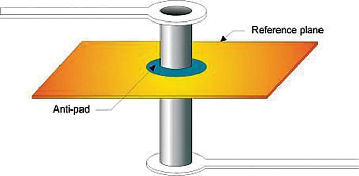
- Keep a watch on the anti-pad. The shape of the anti-pad often affects high-frequency signals. SI analysis can suggest a suitable anti-pad shape for the design under consideration.
- Check no traces or planes are routed in the keep-out areas.
- Make sure the minimum distances specified during layout (for example, the spacing between via to via, via to pad, via to trace, etc) are manufacturable. Contact your PCB fabricator for their capability and cost beforehand.
Happy designing!
Also Read
The author Arka Mukherjee is a postgraduate and gold medallist from IIT Delhi. He is an electronics enthusiast with more than a decade of experience in embedded systems design for optical access networks
