


Time period and frequency are the two most important parameters associated with a wave, may it be analogue or digital. Whereas, frequency is the number of complete cycles of a wave occurring in a specific amount of time (generally a second), time period, on the other hand, is the duration in which a complete wave cycle is achieved. Mathematically the relation can be expressed as T= 1/f, where T is the time period and f is the frequency of a wave.
Oscilloscopes and nowadays digital frequency counters are widely used to measure the frequency of a wave. But, sometimes, it is more advantageous to measure the other parameter, ie. the time period, rather than the frequency. Practically, frequency measurements in the very low frequency range, may produce erroneous result. Moreover, while measuring the width of a pulse, we have to determine the duration of the pulse in time scale, not in number/sec i.e. frequency.
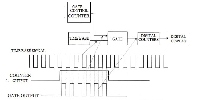
Time period measurement is an inverse process of frequency measurement. While in a frequency measurement, signal of an unknown frequency is allowed to pass through a GATE for a specific amount of time (say a second), a time period measurement, on the other hand, needs the GATE to remain open for a complete time period of the unknown signal. During this time interval, a signal of known time period (we call it “Time Base” signal) sends number of complete cycles to the other side of the GATE, where an event counter counts the number of cycle that reach the other side, and display the result digitally. The number displayed by the event counter multiplied by the time period of the time base signal is the time period of the unknown signal. The time base period must have to be considerably shorter than the unknown period, to have an effective output. Generally, it is in the micro second or millisecond range.

Pulse width measurement applicable to digital signal only. It is an extended application of time period measurement, that requires certain modification in the time period measuring circuit. Let me first concentrate the discussion over time period measurement of an analogue signal.
METHODOLOGY (time period measurement)
Nowadays, digital technics are generally used for the measurements of time period of an analogue signal. The signal whose time period is to be measured may have any shape and amplitude, and as such may not be measured correctly. So, its amplitude is first brought to a fixed level by amplifying or attenuating. The wave shape is then squared up using a Schmitt trigger to convert it to a digital (TTL) signal. The result is a series of TTL pulse, either rectangular wave or square wave in shape. The time period (Mark time + Space time) remains same as the original analogue signal. So, the time difference between any two consecutive pulses is our desired time period of the analogue signal.
Basic Time interval measurING system
A basic system to measure the time period, i.e. time interval between two consecutive pulses coming from the squared up incoming signal is described with the help of a block diagram shown in figure-1 below.
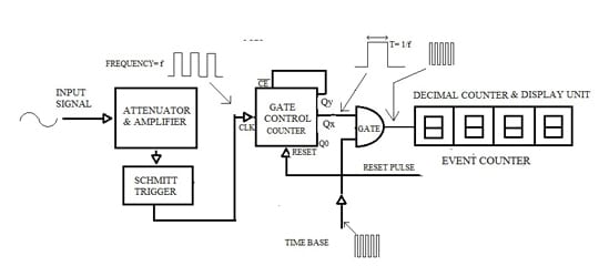
Assume, that Qy output of the “GATE control counter-decoder” is, initially, at high state. Since it is tied up to the CE(active low) input of the counter, incoming signal pulses are inhibited to advance the counter. So, the counter stays in an idle condition with all the other outputs of the counter (including Qx) are at logic 0. Since Qx feeds one input of the GATE, which is a 2-input AND gate, the GATE is disabled and no signal can reach its output side. Now, as soon as a RESET pulse is applied to the counter, Q0 instantly goes high and all other outputs of the counter goes low. Since the status of Qy now changes to logic-0, the CE input of the counter becomes active and allows input signal pulses to advance the counter from Q0 to Qy sequentially.
While the counter advances from Q0 to Qy, each of its output pins goes to logic 1 and stays at that state until a next (consecutive) pulse advances the counter by one step. So, the outputs would stay at logic 1 sequentially for a length of time that is equal to the time period of the input signal. In this process, when Qx becomes high, the input of the “GATE” that is tied to Qx is raised to logic 1.The GATE then outputs the time base pulses fed to its other input. Vide figure 2 for better understanding. The process stops when the next pulse advances the counter from Qx. The total number of pulse that is already allowed to reach the other side of the GATE, is counted by the event counter and display the result digitally using 7-segment LED displays. The number displayed, if multiplied by the duration of each time base pulse (micro second, millisecond etc), gives us the time period of the input signal. The counter goes on advancing with each pulse arriving at its clock input, until Qy becomes logic-1, As soon as Qy becomes high the counter again goes to idle condition. The whole process would be repeated if another RESET pulse is applied to the counter.
System modification for pulse width measurement
Now let us concentrate our discussion over how a time period measuring circuit could be used to measure the pulse width of a digital (TTL) signal. Since, Time period = Mark time + Space time. the duration of the desired high going pulse (i.e. Mark) can be had if we could subtract the “SPACE” duration from the time period, To attain this target the basic system technic used for time period measurement, has to be modified. The modified system is indicated in the block diagram shown in fig.3 below.
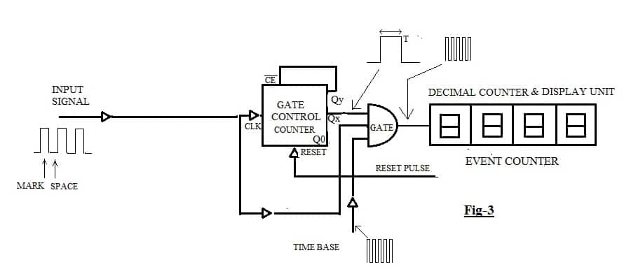 In the modified system, instead of 2-inputs, the GATE possesses 3-inputs. The 3rd one is used to separate the MARK(high going pulse) part of a TTL wave. Here, the function of the GATE depends not only on logic state of Qx, but also on the instantaneous status(MARK or SPACE) of the input signal too. The GATE would now allow time base pulses to pass through it when, and only when the counter output Qx as well as the instantaneous status of the input signal, are both at logic 1 state. This condition is met only during MARK interval of the input signal. So the time base pulses that could reach the output of the GATE is a measure of the high going pulse width, ,i.e MARK.
Block Diagram Of Time Period Cum Pulse Width Meter
Now let us join the blocks already discussed to get the block diagram of the project as a whole. According to the title of the project, the project can measure both the time period and the pulse width in a single unit. The combined block diagram is shown in fig 4 below.
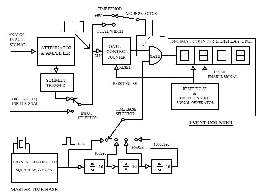
Two, one pole 2 way switches, are used to select either of the two modes. The input selector switch SW1 is used to select either a direct digital (TTL) signal or a analogue signal converted to TTL form. The mode selector switch SW3 selects either time period or pulse width measuring system to be active. A crystal controlled square wave oscillator acts as the time base signal generator. Its frequency is 1MHz and outputs 1uSec time base pulses. The output is again divided by three decade counters connected in tandem to produce time base pulses of 10uSec, 100uSec and 1000uSec respectively. Time base selector switch SW2 can be used to select the proper one, to get effective countable output pulses for a particular input signal. The event counter starts the GATE control counter by sending a reset pulse to the counter, and at the same time resetting the 4 digital displays to “0000”. It then initiates fresh counting by enabling its internal 4 digital counters. They count and display the result digitally on four 7-segment displays.
Circuit Description
Let me now explain the practical circuit for achieving the desired target. The whole circuit is divided into three units-
- The MAIN Unit
- The EVENT Counter (Pulse counting and display section)
- TTL Signal Source
The Main Unit
Fig 5 shows the schematic of the Main unit The MAIN unit comprises 4 blocks.
- The Input Signal Amplifier and squarer,
- The GATE control counter,
- the GATE, and
- The “Time Base Generator”.
.. Let me describe the blocks serially. Time Base Generator first.
Time Base Generator
Master Time Base pulses are generated by a crystal controlled TTL gate oscillator. Two gates (A1 B1 Y1 & A2 B2 Y2) of IC1(74LS00), which is a Quad 2-input NAND gate, are made to act as “INVERTOR” by tying their individual inputs leads(pin 1,2 & 4,5 )together. The said NAND gates are connected in tandem and biased linearly to act as amplifiers with the help of feedback resistors R1 & R2 respectively, connected from output(Yx) to inputs(Ax,Bx). Together, they provide a 360 degrees of phase shift with the feedback path coming from the output (pin 6) to inputs (pin 1,2) of the IC through the crystal. So, as the criteria for oscillation are met, oscillation occurs and output frequency equals the crystal’s resonance frequency, which is, in this case, 1MHz. The capacitor C1 simply blocks DC in the gain path. Oscillator output is buffered by two remaining gates (A4 B4 Y4 &A3 B3 Y3) of the IC connected in tandem. The buffered Time base Pulses are available at pin 8 of the IC. Time period of Master Time Base pulses is 1uSec. To get other time bases, Master Time Base output is divided serially by three “divided by 10 counters(IC2,IC3 & IC4)” to get 10uSec, 100uSec and 1000uSec time bases. Decade counter decoder CD4017 is configured to do the division function. These time bases i.e. 1uSec, 10uSec, 100uSec and 1000uSec are available through switch 5,6,7 and 8, respectively of DIP switch SW2.
Input Amplifier and Squarer
Transistor Q1 is configured to act as a CE voltage amplifier to amplify the analogue signal voltage. Signal whose time period is to be measured is fed to the base of the transistor Q1 via variable resistor VR1 and DC blocking capacitor C1. Variable resistor VR1 acts as the “Attenuator” and is used to control the input signal amplitude before feeding it to the base of the transistor Q1. Resistor R4 and R5 are used for voltage divider biasing of Q1’s base. Capacitor C4 is used to bypass the emitter resistor R7 for AC signal. R6 is the collector resistor across which the amplified signal is developed. The amplified signal is coupled to the input pins 12 &13 of IC5 (CD4093), which is a quad NAND gate with Schmitt trigger. The capacitor C3 is used as the DC blocking capacitor. Transistor amplifier Q1 is used to raise the signal voltage to proper level needed by the Schmitt trigger IC. The level, when measured found to be nearly 1.3V. RMS. The Amplifier needs 15mV RMS (approximately) at its Base to produce the required output signal voltage.
CD4093 (IC5) comprises four 2-input NAND gates with Schmitt trigger. As already indicated above, the amplified (and inverted) analogue signal whose time period is to be measured, is fed to the input pins(12 &13) of the gate (A4 B4 Y4) of the IC. There, the signal is squared up to TTL waveform by the Schmitt Trigger action. It also gets inverted once again by the gate’s NAND function. So, as the input signal has gone through double inversion, first by the transistor and second by the NAND gate, the output at pin 11 of IC5 represents the digital (TTL) form of the original analogue input signal.
Gate & Gate Control Counter
Whereas, quad 2 input AND gate IC7(7408) is configured to functions as the GATE, IC6(CD4017), is used to control the operation of the GATE. IC6 is a decimal counter/decoder IC, and provides 10 separate decoded outputs (from 0 through 9) at Q0 through Q9 outputs of it. The counter advances when clock pulses are applied to pin 14(i.e. CLK input) of the IC, provided that its CE input(pin 13) is at logic 0 state.
Now, let us assume that output Q9 of IC6 is at logic high state. Since CE input(an active low input) of this IC is tied up to Q9, logic state of CE is also at high. So, IC6 cannot advance in counting but stay in an idle state. Now, if a RESET pulse is applied from the EVENT COUNTER to the IC’s RST(reset) input (pin 15), the counter is reset immediately, and all its outputs except Q0 becomes low. Q0 goes to logic high state. Q9, and hence CE input of the IC are now at logic low state. Hence, the counter starts counting the clock pulses coming either from pin 11 of IC5, or from a digital(TTL) source. The choice depends upon the setting of the selector switch Sw1. .
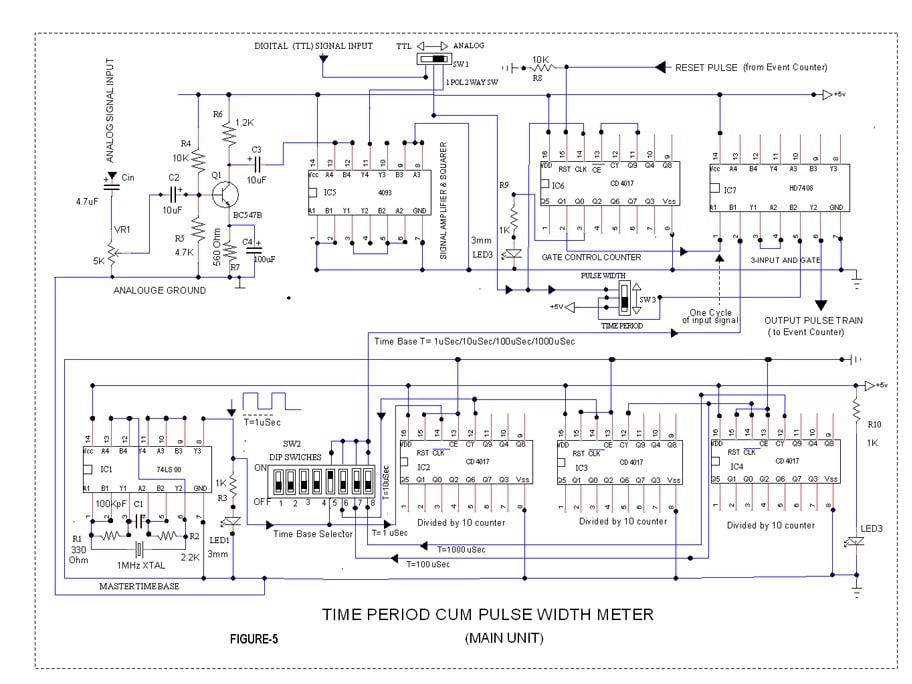 As the counting goes on, each of the outputs of IC6 becomes high sequentially and stays at that high state for a duration that equals the time period of the incoming signal, since the time difference between two consecutive clock pulses of the incoming signal is equal to its time period. In this process when Q9 again becomes high, the counter stops counting and goes back to its idle state. It would stay in this state until and unless the EVENT COUNTER again sends a reset pulse to reset IC6, when the whole process would be repeated once again.
The Gate
It is already indicated above, that IC7 is configured to act as the GATE. 2 gates of IC7(A1 B1 Y1 & A2 B2 Y2) are connected in tandem. Together they become a 3-input AND gate. This AND gate functions as the “GATE” indicated in the block diagrams(vide methodology section). During a counting cycle of IC6, discussed above, when Q1 becomes high, it raises pin 1(A1) of IC7 to high state. Another input of the GATE, pin 2(B1) is fed with Time base pulses via a switch of DIP switch SW2. Depending upon the switch’s setting 1uSec/10uSEc/100uSec or 1000uSec time base is coupled to B1 input of the GATE. Logic state of B2, the third input of the GATE depends upon the setting of the switch SW3. When it is sled to “Time period” side, IC7 becomes a 2-input AND gate as pin 5 of IC7 is pulled up to +5V by the switch. On the contrary, when it is set to Pulse width side, pin 5 becomes free and makes the GATE a 3-input AND gate. Incoming clock pulses now gets applied to this pin too via SW3.
When the GATE is made to act as a 2-input AND gate, by sliding SW3 to “Time Period Side, the GATE allows selected time base pulses to reach its output i.e. pin 7 of IC7, so long the output of IC6 (pin 2) remains high, i.e. during the time period of the incoming signal. The pulses go to the event counter (pin 1, IC12) for counting and display.
Pulse width measurement.
If the switch SW3 is sled to “Pulse Width” side, pin 5 of IC7 gets connected to input signal pulses through switch SW1, as indicated above. So, “Time base pulses” would be allowed to pass to the output of the GATE (pin 7 of IC7) only during the “MARK” period of the incoming signal, as explained previously in the Methodology section. So, the number of pulses that would be counted by the event counter, in this case, would represent the “Pulse width” of the incoming signal
THE EVENT COUNTER (Pulse Counting & Display Section)
Fig 6 shows the schematic of the EVENT COUNTER. For proper indication of the measured time interval (time period or pulse width), the time-base pulses coming out of the GATE (IC7) of the main unit must have to be counted properly. To have this goal reached, a 4-digit event counter is constructed using discrete digital ICs, and 7-segment displays. The counter can count and display up to 9999 pulses. Depending upon the time-base unit selected in the MAIN unit (using SW2), this corresponds to 9999 micro Seconds through 9999 milli Seconds, or 9.9 Secnds.
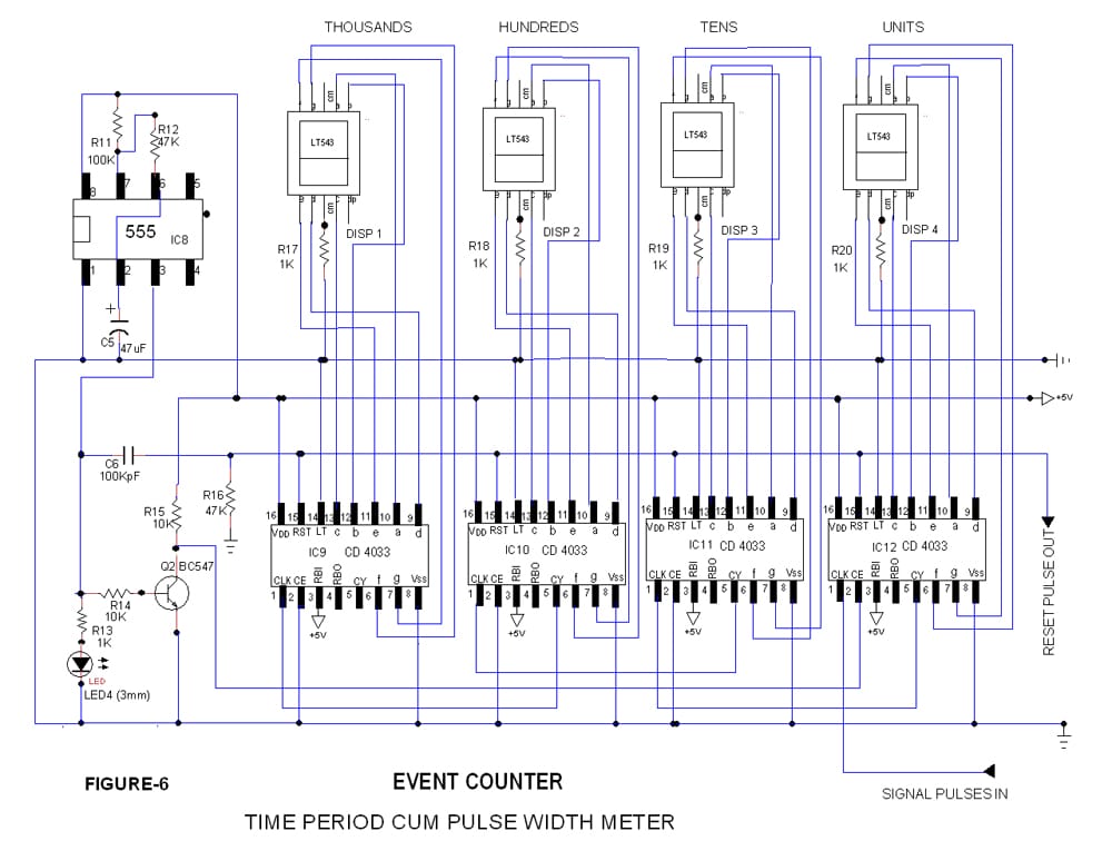 Circuit Description of the Event counter
Four CMOS decade counters cum 7-segment LED drivers are connected in tandem to form a 4-digit decimal counter. CMOS digital IC CD 4033 is used for this purpose. The Pulse Train coming out of the GATE(i.e. through pin 6 of IC7) is fed to pin 1(CLK input) of IC12(4033). Its outputs drive the Display-4( a 7-segment LED display). If pin 2 (CE input) of IC 12 is at logic 0, each pulse from the IC7 advances the counter by 1. The logic condition of pin 2 is dependent upon the collector voltage of transistor Q2, which is again dependent upon the output logic condition of the astable multi constructed around IC8(555). The time period of the astable is governed by the combination of resistor R11, R12 and capacitor C5. It generates asymmetrical square waves with T high is much greater than T low.
Whenever pin 3 (output) of IC8 goes to high state(logic 1) it would do two functions. Firstly, the high going pulse resets all the decade counters (IC9-IC12) of the EVENT COUNTER and the “GATE control counter” IC( IC6) of the Main unit. It resets through capacitor C6. Secondly, it pulls down the collector of transistor Q1 to logic 0 state. The transistor Q1 would stay at this state so long IC8 output is high( approximately for 6 Seconds). So, the logic state of CE input (pin 2) of IC12 would also be dragged and remain dragged to logic 0 state for the same duration. Now IC12 and 3 other counters(IC11, IC10 and IC,9) connected in tandem, start counting the pulses fed to pin 1(CLK) input of IC12. The pulses are fed from pin 6 of IC7. After the T high state of IC8 is over, Q1 returns to its normal state dragging CE input of IC 12 to logic high state, prohibiting further counting. The number of pulses counted so far, would be displayed as 4 digit decimal number by the four 7-segment displays in the following manner. Units by Display-4, Tens by Display-3, Hundreds by Display-2 and Thousands by Display-1 respectively..
The display would stay stable until and unless IC8 again resets the display counters and IC6. A new series of pulse would then arrive from the main unit for fresh counting and display. The process would go on repeating so long the power supply is connected to the circuit, and there is an input signal.
The time period of the astable multivibrator constructed around IC8 should be such that it allows at least 5 pulses of the input signal to be fed to IC6, so as to get stable display for easy viewing.
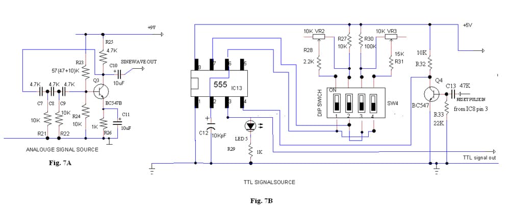
TTL Signal Source
A digital(TTL) signal source is developed to ease the testing of the project. The related circuit is shown in Fig-7B. A 555 Timer is configured to function as an astable multivibrator. Two switchable sets of resistances are used to produce two different time periods with the help of capacitor C12. Whereas the first set comprises R28 and (R27+VR2) combination, the second set comprises R30, R31 and VR3 as frequency determining network.. VR2 and VR3 are two multi turn Trimmer potentiometers. Selection of first or second set is done by way of 4 way DIP switch SW4. Output frequency and hence time period can be varied by varying VR2 or VR3, which one is selected. By precisely adjusting the trimmer pots, one set can be made to produce time period which would be 10 times of the time period that is produced by the other.
The TTL signal source shown in fig.7B can also be used to evaluate an unknown capacitor. In an astable multivibrator, constructed around a 555 Timer IC, the capacitor “C” is related to ‘T” (the total time period), and resistors(RA, RB) by the formula-
C=T x 1.44/(RA+ 2RB).
Here, if RA(R27) and RB(R28+VR2) are chosen as 10K and 2.2K respectively, the term 1.44 vanishes out from the formula and the formula gets simplified to
C(pF)=T(uSec) x 100 .
Similarly if R30 and R31+VR3 combination are 10K and 2.2 K respectively, the formula comes out to be
C(pF)=T(uSec) x 10.
So, by using the appropriate formula( which depends upon the setting of SW4), we can measure the capacitance of a capacitor, by merely reading the time period from the display.
Synchronization
The timer can be synchronized with output of IC8. For which, output of IC8(pin3) is to be connected to the base of the transistor Q4 via capacitor C13. Q4 normally remains OFF. So the RESET input of IC13 stays at logic 1, allowing the timer to oscillate on its own. As soon as IC8 output goes high, it sends a high going pulse to Q4 base, turning the transistor ON for a brief moment. Its collector voltage drops to reset the timer IC13. During measurement of a large capacitor (say 500uF), this resetting is required to display a stable correct capacitance value.
Construction and Testing
The prototype of the project is assembled and tested on two separate IC bread boards, one for the Event Counter unit and the other for the Main unit. TTL signal source is mounted on a separate breadboard. Alternatively, it may be constructed on general purpose IC Vero boards, or on a specially designed PCB made for this particular project. During construction, one point must be remembered carefully that the amplifier ground (analogue ground ) must be returned separately to the supply ground, otherwise circuit may start malfunctioning. A phase shift oscillator shown in Fig-7A may be constructed to act as an analogue signal source.
Testing the EVENT COUNTER ( Pulse Counting and display section)
Connect a +5V supply to the circuit. Switch ON the supply. LED 4 should start blinking immediately. Connect a small wire to pin 1( signal input) of IC12(4033). Connect the other end of the wire to ground. The 4 displays should now show ‘0000’. Now disconnect the wire from ground. The last two displays(Thousands and Hundreds) should continue to show “00” as before, but the two other displays (Units and Tens )should go on counting continuously to show a two digit random number.
Testing the MAIN Unit
To test this unit we must have in hand a good working EVENT COUNTER. Complete all the interconnections between the EVENT COUNTER and the MAIN unit. RESET pulse output line from the junction of R16 and C6 in the EVENT COUNTER, is to be connected to the junction of R9 and pin 15 of IC6, in the Main unit. Pin 6 of IC7(Pulse Train output). is to be connected to Pin 1 of IC 12.
Connect a +5V supply to both the sections. A glowing LED1 indicates well functioning of the crystal time base generator. Now Slide the switch SW1 to “TTL” side and SW3 to “Time period” side. Next, slide switch 5 of SW2 to ON. Connect a jumper from TTL input to CY output of IC4(CD4017). The display should now show “1000” along with a blinking LED 3. Since it blinks very sharply, you may have to notice it very carefully. Blinking of LED 3 indicates proper functioning of the GATE CONTROL counter(IC6) & the EVENT COUNTER. The display “1000” indicates proper functioning of the Time base Generator, and the 3-input ”GATE” constructed around IC7.
Testing of TTL signal Source
Replace C12 with a 1uF capacitor. Slide switch 3 &4 of SW4 to ON. Connect a +5V supply to the unit. LED 5 should start blinking immediately.Now connect the TTL output coming out of IC13 (pin 3) to the TTL input of the Main unit. Throw switch 8 of SW2 to ON to select Time Base=1000uSec. The display should now show a value close to 1000.
Adjustments of VR2 and VR3
Connect a known value capacitor (say 820 pF) in place of C12. Change C5 to 10uF. Slide switch 3&4 of SW4 to ON, if not done already. Select Time Base= 1uSec by sliding switch 5 of SW2 to ON and all other to OFF. The display should now show a value close to 0082, means 82*10*1 pF or 820pF. If display differs, adjust VR3 carefully to get a display of 0082
Now replace C12 with another known value capacitor(say 100KpF). Make switch 1&2 of SW4 ON and switch 3&4 OFF. Select Time Base=10uSec by sliding switch 5 of SW2 to ON. The display should show a value close to 100 means 100*100*10 pF or 100KpF. Adjust VR2, if required, to get proper display.
. Synchronization is not must in these cases. So Q4 base may be kept floating.
Applications
Apart from measurement of time period and pulse width of an unknown signal, the circuit is best suited for testing the performance of an Oscillator or multivibrator.
Finding Duty Cycle
By measuring the Time Period and Pulse Width of a digital signal, we can easily calculate to find out another important parameter of digital wave, the Duty Cycle.The Duty Cycle “D” of a digital signal is expressed by the formula,
D= (Pulse Width)/(Time period).
Testing of Capacitors
As indicated earlier, the TTL signal source can be used to evaluate an unknown capacitor. The range, however, limited. It can be used to measure a capacitance value if it lies in the range of 10 pF to 1000uF. To show a value greater than 100uF, C5 is to be increased adequately. The meter would take more time to display the result. By increasing C5 to 100uF, capacitance value more than 500uF can be tested. Output of IC8 has to be connected to C13 to synchronize the function of IC13.
For stable display, Time Base should be selected to 10 or 100 or 1000uSec, whichever is appropriate, to fit the number within 4-digits. The displayed value, after multiplying by 10 or 100, depending on the setting of SW4 of TTL source, is to be multiplied further by 10 or100 or 1000 depending on the time base selection, to get the value of the capacitor in pF.
To measure a capacitor follow the steps below.
Connect the unknown capacitor in place C12. Make switch 3 &4 of SW4 ON for capacitors lying in the pF or KpF range. On the other hand , Switch 1&2 are to be used in the uF range. The display should immediately show a random number. Wait for LED 4 to blink once again. The display should now show a stable number. The last two digit ( Tens & Units) may show a changing value after each blink of LED 4, which is normal. Multiply the displayed number by the Time Base used, to get the value of the capacitor in Pico farad(pF). For an example, if the switch 3& 4 are ON and selected Time base is 10uSec and Display shows 470, the capacitor value is 47000pF or 47KpF.
 Stray capacitance imposes a problem in measuring a capacitance value lower than 100pF. However, a lower value capacitor (say 20pF) may be measured with the help of another capacitor(say 820pF). First, replace C12 with a 820 pF capacitor. Note the number being showed on display ( say 82). Now connect the unknown capacitor ( say 20pF) in parallel to 820 pF. A 20pF in parallel to a 820pF should produce a display of 84.
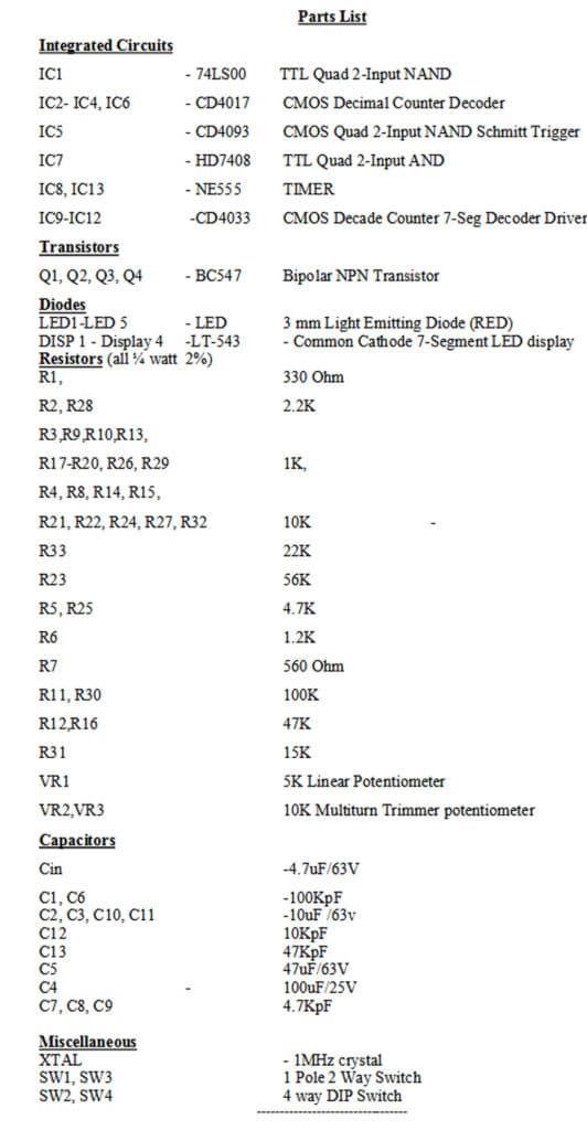
Arup Kumar Sen Ex-Technical Officer-II Bose Institute Kolkata