


Introduction
In July 2021 issue of EFY magazine, article “Solar Pooja Lamp That Runs Nonstop” was published. It uses supercapacitors to power LEDs in the night. In FEB 2023 issue of EFY, “POWER SUPPLY FOR A CLOCK Using Supercapacitor And Small Solar Panels” was published.
Here, an improved Pooja Lamp is proposed with 32 extra LEDs (5 mm 20 mA) to get more light in the day time. Further, clock power supply circuit is integrated, which drives two wall clocks. The power supply circuit draws power from the same PV panel used for Pooja Lamp.
System runs non-stop for 15 years without needing much attention. It can conserve edible oil and eliminate AA batteries. This is a very cost-effective and attractive combination and is expected to boost demand for supercapacitors.
Improved Pooja Lamp
Circuit diagram of improved Pooja Lamp is shown in Fig. 1. It consists of two PCBs. PCB_L for Left lamp and PCB_R for Right lamp. In each PCB, one 500 F supercapacitor is accommodated. These PCBs are mounted at the bottom section of two silver lamps. For interconnections between the two PCBs, 8 pin polarized headers (CON_L, CON_R) have been used. A 10 W Solar PV panel (17.5V Vmp, 580mA) is used to power the circuit.
Note that, in the circuit diagram the screw terminals are shown by black bullets. The signals going to the 8 pin headers are shown by triangles. Table 1 shows the interconnections between CON_L and CON_R. The jumper cable is made by doing one-to-one pin connections using two 8 pin housings.
| Node Identifier | EL+ | EL- | A | B | Vc | JL+ | JL- |
| Node Identifier | ER+ | ER- | A | B | Vc | JR+ | JR- |
| CON_L, CON_R pins | 1 | 2 | 3 | 4 | 5 | 6 | 7, 8 |
Table 1 shows the interconnections between CON_L and CON_R.
Recap of Pooja Lamp
LED1 to LED10 are 1 W orange LEDs which turn ON during day time. Five of these LEDs are connected in series for each lamp and their current is limited by resistors R1 and R2 (27Ω 1W). The current flowing through these resistors flows through D1 (1N5819) and charges supercapacitors C1 and C2 (500 F 2.7V). Resistor R3 (0.33Ω) and Zener Diode ZD1 (2.7V 1W) limits the supercapacitor voltage to 2.7V. Also, diode D2 (1N5819) and D3 (6A4) and LED11 to LED26 (Orange 5mm 20mA) prevent C1 and C2 from getting overcharged. Note that, all these 16 LEDs are connected in parallel (OM) and these turn ON only when the supercapacitors are fully charged. Charging time of these capacitors may range from 2 to 4 hours depending upon the sunlight intensity.
In the night, the energy stored in the capacitors is used by the Joule Thief circuit made using transistor T1 (BC547C), and Toroidal transformer TCT1 (50:50 turns, 32 mm diameter). It powers LED27, LED28 and LED29, LED30. These LEDs are 5mm 20 mA superbright white LEDs which maximize light output. In the day time, the PV voltage sensing circuit consisting of transistor T2 (BC546), resistors R5 (6.8kΩ) and R6 (1kΩ) stop the joule thief circuit from oscillating. When PV voltage does down in the evening, the Joule Thief circuit starts functioning.
Tips for Toroidal Transformer: For the primary winding, a thicker enameled wire is recommended, eg SWG 20. For secondary a very thin wire can be selected eg SWG 30. This will ensure that both windings could be wound in single layer. Also, we can increase the number of turns up to 80 turns. (primary and secondary number of turns should be equal). Increasing the number of turns will slightly reduce losses in T1.
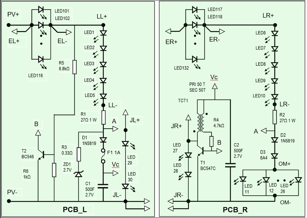
Fig.1 Circuit diagram of improved Pooja lamp with 32 extra LEDs.
Extra LEDs
LED101 to LED132 (Green 5 mm 20 mA) are all connected in parallel. These are grouped in two rings of 16 each. One ring is mounted on the left lamp, the other on the right lamp. These LEDs are inserted between PV+ and LL+ (and LL-) nodes. Which introduces forward voltage drop of one LED. Even after inserting these extra LEDs, the performance of original pooja lamp is not affected. The reason being, PV panel voltage increases by forward voltage drop of one LED, because PV panel acts as current source. The Pooja Lamp voltage remains same for given intensity of solar radiation.
Equation for PV voltage when C1 and C2 are fully discharged is as follows:
Vpv = VLED(G) + [5 * VLED(Or)] + VR1 + VD1
18V = 2.75V + 5 * 2.1V + VR1 + 0.3V
Drop across R1 = VR1 = 4.45 V
Current through R1 = 4.45V / 27Ω = 165 mA
Similarly, 165 mA current flows through R2.
Current through individual green LEDs = 165/16 = 10.31 mA
Thus, current in each green LED is about 10 mA. Which is within the max current rating.
Selection of Extra LEDs: Since all 32 LEDs are connected in parallel, it is necessary to ensure that all these LEDs have matching forward voltage. So that all LEDs will provide uniform light intensity. In this design, green LEDs have been selected. However, user can select any other color. The forward voltage of individual LEDs can be measured by making a simple test circuit. To a 5 V adaptor positive terminal, connect 220Ω current limiting resistor on a bread board. Connect LEDs between resistor and the ground, one by one and measure the forward voltage of each LED. Group the LEDs having same forward voltage. A small variation of ± 0.1 V is acceptable.
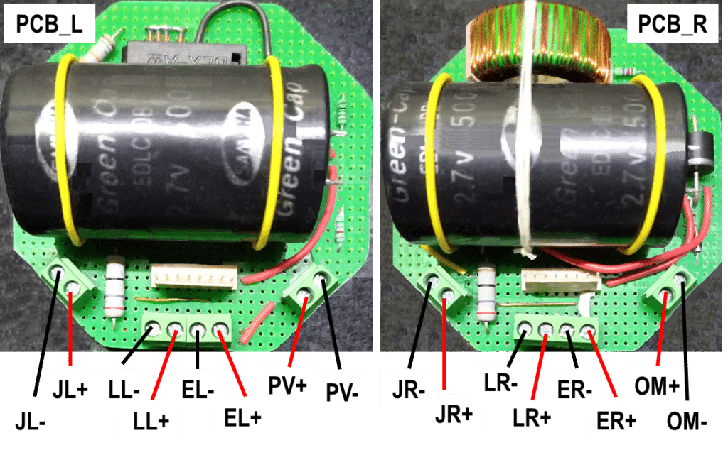
Fig.2 Two PCBs for mounting inside two small silver lamps.
Figure 2 shows two assembled PCBs with one supercapacitor mounted on each of them. The screw terminals are soldered on one side of the PCB. The various connections to be made to these terminals have been identified. 8 pin headers are soldered to each of the PCBs for interconnections between the two PCBs. These PCBs are mounted in the cavities at the bottom section of small silver lamps. For connections to the LEDs mounted on the lamp, use of very thin (7/42) white wires. These are easily available in the market.
Single Lamp
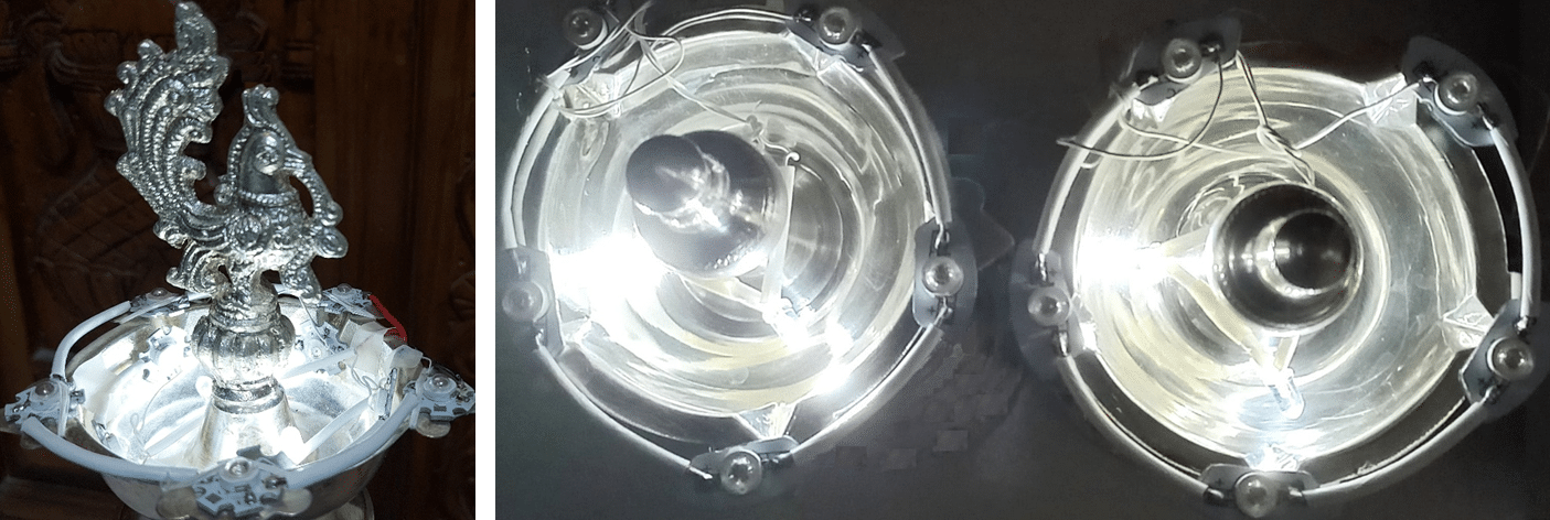
It is possible to make one single bigger lamp to accommodate the full circuit of Fig. 1. In this case, the 8 pin headers are removed and the nodes identified in each column of Table 1 are shorted. Fig 3 shows the photograph of single PCB design. Note that nodes LL+ and LL- merged and named as L+. Similarly, EL+ and ER+ merged as E+, EL- and ER- merged as E-, JR+ and JL+ as J+.
Fig 4 shows the two supercapacitors assembled lengthwise and connected in parallel. This assembly is mounted in the vertical space available at the bottom section of the big lamp. PCB is fixed at the base so that capacitor assembly gets support at the center of this PCB.
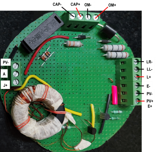
Fig.3 PCB for single big lamp. Space at the center of PCB to accommodate supercapacitor assembly.
Fig 5 (a) shows the big lamp with all the day light LEDs turned on. Two rings of green LEDs are mounted on the bottom section of this lamp. Fig 5 (b) shows two small lamps with the day light LEDs turned on. For each lamp one green led ring is mounted at their bottom sections.
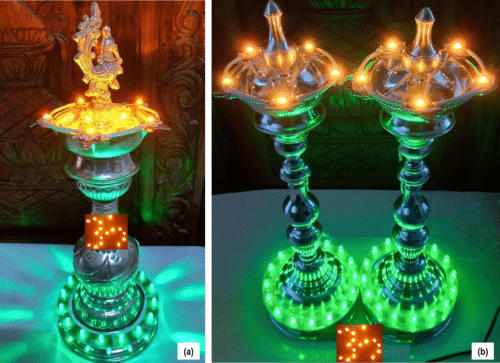
Fig.5 (a) Single big lamp with 2 green LED rings at the bottom. Fig.5 (b) Two smaller lamps with one green LED ring at the bottom.
Fig 6 shows white LEDs turned ON during night, with the help of joule thief circuit. On the left side, single lamp has 4 white LEDs. On the right side, for the two lamps 2 white LEDs each are ON.
Integration of clock power supplies
As mentioned in the article on Clock Power Supply, the wall clocks need very small power. Which can be tapped from the PV panel used in the Pooja Lamp. I addition, we need a supercapacitor to drive the clock during night. However, we can not use the supercapacitors used in the Pooja Lamp. The reason being, the joule thief circuit utilizes all the energy stored in these capacitors through out the night. The capacitor voltage in the early morning drops below 1 volt. Clock minimum working voltage is 1 volt. Hence, we need to use a dedicated supercapacitor for the clock driver circuit. The design of this circuit is given below:
Design of Clock1 power supply
Figure 7 shows the power supply circuit for the Clock1. It consists of a supercapacitor C101 (100F 2.7V). It is connected through diode D101 (1N5819) to node A of the Pooja Lamp circuit (see Fig.1). Node A supplies charging current to C101. Also, the over charging protection circuit consisting of D1 & ZD1 and D2, D3 and LED11-LED26 also provides protection to C101 against overcharging.
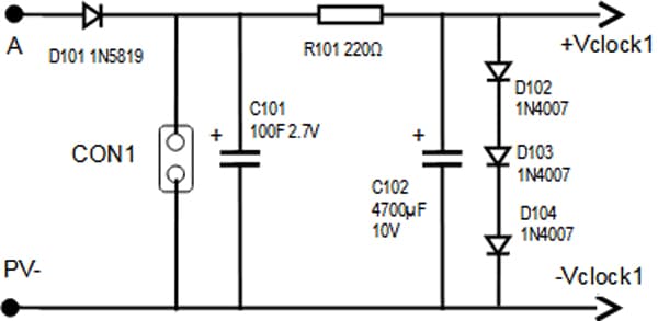
Supercapacitor is connected to the +Vclock1 terminal through current limiting resistor R101 (220Ω). A filter capacitor C102 (4700µF 10V) is connected across the clock terminals. Diodes D102, D103 and D104 (1N4007) are also connected to clamp the voltage below 2V. Across C101 a 2 pin polarized connector header CON1 is connected. This connector provides power to the second clock driver circuit as explained below.
Design of Clock2 power supply
Figure 8 shows the circuit diagram of Clock2 power supply circuit. It consists of 2 pin connector header CON2. A 2 pin jumper cable is used to tap the power from Clock1 PCB to Clock2 circuit. Current limiting resistor R102 (220Ω) is connected from CON2 to +Vclock2 terminal of the second clock. Also, filter capacitor C103 (4700µF 10V) and clamping diodes D105, D106 and D107 (1N4007) are connected across clock2 terminals. Note that this circuit uses the energy stored in C101. There is no need of additional supercapacitor for Clock2, thus reducing the cost and size of this PCB.
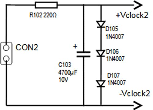
Fig.8 Circuit diagram of Clock2 power supply without supercapacitor.
Fabrication and Interconnections
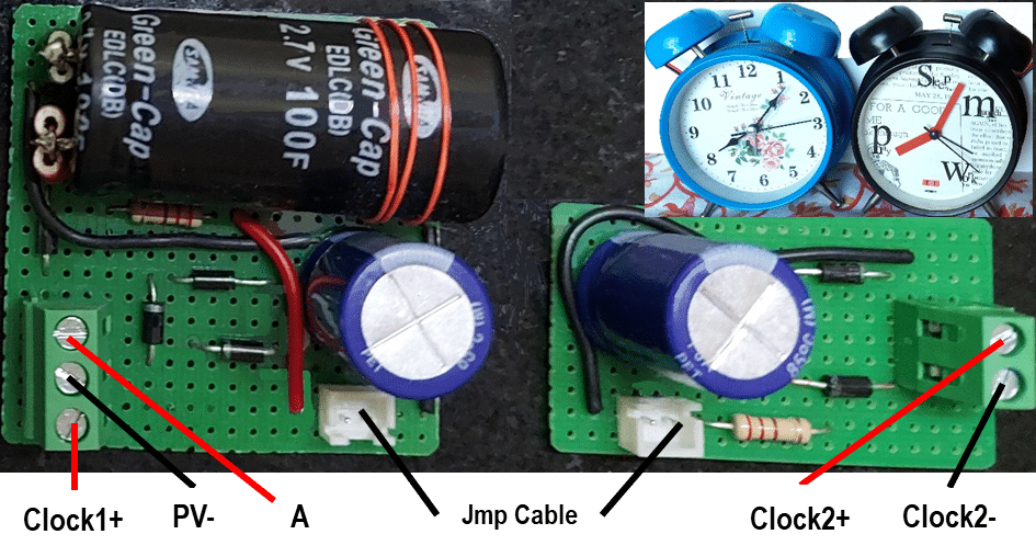
Figure 9 shows the assembled PCBs for Clock1 and Clock2. These PCBs have to be kept near to the respective clocks because the filter capacitors should be close to them. Run a cable from terminals A and PV- (see Fig. 3) to the respective terminals of Clock1 PCB. There is no restriction on the length of this cable. Make a 2 pin Jumper of required length and interconnect the two PCBs. Again, there is no length restriction for this jumper cable. Connect the outputs of these PCBs to respective clocks. For making all these cables very thin wires (7/42) can be used, which are easy to conceal.
Conclusion
An integrated system consisting of Solar Pooja Lamp and Clock power supplies is proposed here. It uses supercapacitors to store energy, for powering the lamps and clocks during night time. These capacitors can handle daily charge and discharge cycles and are environment friendly. They have 15 years of life. This integrated system can find use in every house and has potential to save large amount of cooking oil and eliminate AA cells throughout the life of the clocks. This will eliminate hazardous chemical waste. The user will have the satisfaction of using solar energy in their homes.

Sir,
Thank you for the circuit using green and clean energy. Well done. Much appreciated!
You are most welcome