


Do you want to design a mobile charger that can charge your phone at a super-fast speed?
The Texas Instruments reference design is a single-cell Li-ion charger reference design which uses a dual charging IC configuration to achieve a fast charge with low heat dissipation. When powered by an optimal 12 V source, the charger can provide a charging current of up to 5A with a low thermal budget. The reference design has an efficiency of up to 94%. The circuit design has been tested by TI and uses the EVM GUI and getting started guide.
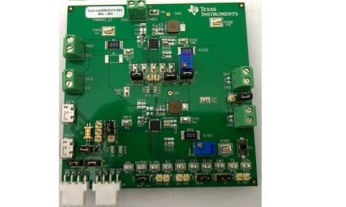
Fast charger reference design by TI

Resources
Texas instruments have provided multiple resources such as a BOM, Schematics, CAD files and Gerber files to simplify the design and adoption of the fast charger. You can view and download the resources by clicking on the links given below:

BOM – Complete listing of design components, reference designators, and manufacturers/part numbers
Schematics – Complete listing of design components, reference designators, and manufacturers/part numbers
CAD/CAE files – Files used for 3D models or 2D drawings of IC components
Gerber files – Design file that contains information on physical board layer of design PCB
The reference design utilises 2 charging IC marked as U1 and U2 in a dual IC configuration. The dual chargers can provide more than their 5 A maximum charge currents and distribute the heat loss across the board more efficiently. The charging IC bq25890/2 is a highly-integrated 5-A switch-mode battery charge management and system power path management device for single cell Li-Ion and Li-polymer batteries. To achieve higher efficiency, the module offers a low impedance power path, which also reduces battery charging time while extending the battery life during discharging phase. The IC also integrates Input Current Optimizer (ICO) and Resistance Compensation (IRCOMP) to deliver maximum charging power to the battery.
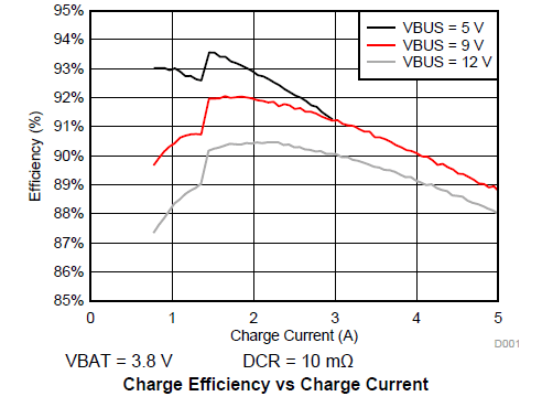
The module is over 90% efficient and has a maximum efficiency of over 94%. The efficiency of the charger decreases as the charge current is increased. The charge efficiency vs the charge current graph of the reference design is shown in the image below:
This device support various input sources which include a standard USB host port, USB charging port, and USB-compliant adjustable high voltage adapter, furthermore, it uses MaxCharge handshake using D+/D– pins and DSEL pin for USB switch control. The device complies with USB 2.0 and USB 3.0 power specs with input current and voltage regulation.
The charger offers multiple safety features which include battery temperature negative thermistor monitoring, charging safety timer and overvoltage/overcurrent protections under-voltage protection, over-discharge protection, etc.
Protection features
The TI reference design comes with multiple protection features which are listed below:
- BAT temp thermistor monitoring (JEITA profile)
- BAT temp thermistor monitoring (hot/cold profile)
- IC thermal regulation
- Bad adapter detection
- ICO (Input Current Optimization)
- IINDPM (Input current limit)
- Input OVP
Features
- Fast charge a smartphone on PCB with a low thermal budget
- Charge currents > 5 A
- This circuit design is tested and uses the EVM GUI and getting started guide
- High efficiency
- Integrated ADC
- Power Path
- USB C/PD compatible
- USB D+/D-/BC1.2 integrated
- USB OTG integrated
- Operating voltage 3.9V-14V
- I2C communication
- LED indication for status signals
- Test points for key signals available for testing purposes
- Jumpers for different circuit configuration
Applications
The module is suitable for mobile phones, cameras, tablets, stand-alone charger applications, etc.
You can find all the resources for TIDA 00590 here.
