


LM1875 is a low cost and very popular and useful integrated circuit (IC). It is designed to be stable with gain higher than ten. Its main application is stand alone audio power amplifier but with two or more additional transistors we can obtain configurations adaptable to more applications. Presented here is a LM1875 based simple amplifier for various applications.
LM1785 IC operation
If the load capacitance is large, e.g. above 1uF it is recommend connecting with series with output of the IC resistor above 1Ohm with appropriate power dissipation. Otherwise the IC may begin to osculate. Another method of driving high capacitive loads is to connect resistor around 10Ohm in parallel with high current inductor of 3-10uH between the output of the IC and the highly capacitive load.
LM1875 is limiting the output current to around 4A but from practical considerations as power dissipation it is good to use maximal output current up to 2A. LM1875 has maximal power supply of +-30V. Usually there is no need to add protection diodes to the output of the IC. Nevertheless two additional diodes (D1 and D2) as shown of Figure 1 can be useful for addional safety precautions. When the temperature of the IC exceeds +170C the IC shuts down.

It is operational again when the die temperature drop to around 145C. The thermal resistance junction – case is 3C/W. The gain product bandwidth of the IC is typically 5.5MHz. The typical slew rate of LM1875 is 8V/us. The maximal output power of the IC is typically 25W over load of 8Ohm at power supply of +-25V.
LM1875 Based Simple Amplifier
Figure 1 is showing the circuit of the LM1875 based simple amplifier. It can produce more than 120W of output power. The amplifier it built around LM1875 and has several configurations over the same printed circuit board (PCB).

The modularity of the solution can provide at least four possible configurations. C3 and C4 are obligatory in all configurations.
1. In the simplest case, IC will work alone and only C5 and C6 from the large filtering capacitors. In that case the output power is determined only from the IC, the size of the heat sink and the power supply and can go up to around 25-30W. The load resistance is 4 Ohm or above.
2. In the second case, IC will work with couple of output transistors, e.g. Q1 and Q4. The filtering capacitors should be at least C5 C6, C7 and C8, each of them for 2200-4700uF/35V. In that case the output power can go to more than 60W and load resistance can be 3.2Ohm and some times below.
3. In the third case, IC will work with four output transistors, e.g. Q1, Q2, Q4 and Q5. In that case it is preferably to use at least six from the the filtering capacitors, e.g. C5 to C10. The output power can go to more than 100W and load resistance can be as low as 1.6Ohm (preferably no less than 2Ohm).
4. In the fourth case, IC will work with all output transistors Q1 to Q6. In that case it is preferably to use all large filtering capacitors C8 – C14. The output power can go to more than 120W and load resistance can be as low as 1.6Ohm.
In all possible configurations the power supply is limited by the power supply rating of the IC. As mentioned above the limits are +-30V and preferably up to around +-28V.
Circuit: LM1875 Based Simple Amplifier
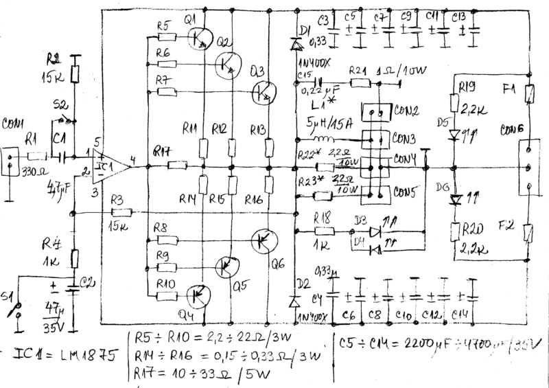
Also in all cases the IC and the transistors should be mounted on the same heat sink and the thermal protection of the IC will protect to some degree the transistors. All transistors do not work with initial (quiescent) current and are blocked at very low level of the output signal and that is reducing the dissipating heat. The short circuit protection of the amplifier is not very important when the amplifier is in the box with the loudspeakers.
That is why the usage of two fusible F1 and F2 can be considered enough for that amplifier. The size of the fusible F1 and F2 in the power supply depends on the maximal current required from the amplifier and from the total size of all filtering capacitors on the board. F1 and F2 can be for 4 to15A and sometimes more. The gain of the amplifier is equal to
G = 1 + R3/R4
and should have the minimal possible value.
That will keep the THD and IND to low level. The loads are connected to the connectors CON2 to CON5. The resistor R21 should be below the load resistance and with appropriate power dissipation. R5 to R10 are obligatory and should have the minimal possible values (usually 10Ohm/2W). R11 to R16 are obligatory and also should have the minimal possible values (usually 0.15Ohm/3W)
Output transistors
This LM1875 based simple amplifier can work with wide variety of output transistors. The output current and output power of the amplifier depends on the selected transistors and the cooling devices.
It is preferably to use transistors with
* maximal continuous collector current above 6A,
* maximal collector-emitter voltage above 60V,
* maximal power dissipation at +25C above 65W,
* transit frequency above 2.5MHz,
* h21e above 20 at large collector current (e.g. above 5A) and
* maximal working temperature more than 150C (preferably 200C).
Appropriate couples of transistors are:
BD907 (NPN) + BD908 (PNP),
BD909 (NPN) + BD910 (PNP),
BD911 (NPN) + BD912 (PNP),
2N3055 (NPN)+ MJE2955 (PNP),
TIP3055 (NPN)+ TIP2955 (PNP),
MJE3055 (NPN) + MJE2955 (PNP)
2SC5200 (NPN) + 2SC1943(PNP),
MJL4281A(NPN) + MJL4302A(PNP)
2N3773 (NPN) + 2N6609 (PNP)
BD249 (NPN) + BD250 (PNP),
TIP33C(NPN) + TIP34C(PNP)
TIP35C(NPN)+TIP36C(PNP),
TIP41C (NPN)+ TIP42C (PNP),
and similar or better.
AC and DC operations
The amplifier from Figure 1 can work as AC and DC amplifier. When switches S1 and S2 are closed the amplified is working as DC amplifier. When switches S1 and S2 are open the amplifier is working as DC amplifier.
Heat sink
The amplifier should work in all cases with appropriate heat sink, e.g. with thermal resistance below 0.7C/W. It is preferably to apply small fan (e.g. 12V/0.1A – 0.3A) over the heat sink in order to improve the cooling. The fan should be activated when the temperature of the heat sink is higher than 50-60C.
Power supply of the amplifier
The amplifier can work with power supply in the full power supply range of LM1875.
The power supply can be regulated or not regulated and should be selected according to the configuration of the amplifier for a particular application.
Construction & testing
For testing and experimenting purposes we in need of power AC or DC amplifier with low cost and easily reparable. In these cases the THD and the IMD of the amplifier are not very important. It is important to have simple solution of power amplifier which can be adapted to a particular application with external passive filters at the input and the output.
Also it is interesting to use the same amplifier with different configurations of elements (kind of modularity or configurability) as output transistors, filtering capacitors, type of the heat sinks, etc. to adapt the implementation to different field of application.
Advantages of the amplifier
Although there are ICs providing similar and sometimes higher output power this LM1875 based simple amplifier with output transistors from Figure 1 has several advantages:
* The total maximal power dissipation of the transistors is higher than the power dissipation of the IC providing similar output power;
* If damaged one or more output transistors can be replaced easily because they have only three pins.
* The maximal output current (both DC and AC) of the amplifier with transistors can be significant, e.g. more than 15A.
* The maximal working temperature of the transistors can reach 200C (for most of the ICs it is around 150C),
* The amplifier can work with many popular and low cost transistors,
etc.
Feel interested? Check out other electronics projects.

Polarity of the capacitor C6,C8,C10,C12,C14 are wrong. In this circuit positive terminal of the capacitors are connected to the ground (-ve) pin.
Need to add Crossover distortion network in before transistor stage. This circuit won’t amplify signals between +0.7v to – 0.7v which is fed to base of transistor.
İn audio power amplifiers,the output stage have to work at AB class.There is no bias cırcuıt ta achieve AB class.With these condition this can only work for power inverter.
LM1875 delivers POUT=20W, RL=4Ω, fo=1 kHz with 0.022% THD.
What is the additional distortions contributed by the external PNP and NPN transistors?