


 Presented here is a memory design project using Verilog hardware description language (HDL). This project is simulated using ModelSim software, and the design is tested through a simulation process. Simulation is done to check, verify and ensure that what is wanted is what is described.
Simulation is carried out through dedicated tools. With every simulation, the results are studied to identify errors in the design description. Errors are corrected and then another simulation is carried out. Simulation and changes to design description together form a cyclic iterative process, repeated until an error-free design has evolved.
Design description is an activity independent of the target technology or manufacturer. It results in a description of the digital circuit. To translate it into a tangible circuit, one goes through the physical design process.
The same constitutes a set of activities closely linked to the manufacturer and the target technology. For designing projects in HDLs, you have to follow the very large-scale integration (VLSI) design flow and verification steps required in each step.
Single-port Memory
The single-port memory is basically the design as per your defined specifications. Then, as per the specified width and depth, define the memory block that can also be verified using field programmable gate array (FPGA) boards. Design hierarchy also plays an important role in designing the basic building blocks required in each step of verification.
In this project we design a 64-bit x 8-bit, which is a single-port design with common read and write addresses in Verilog.
While designing this project in ModelSim and test benches, follow the guidelines mentioned below:
1. When modelling sequential logic, use non-blocking assignments
2. When modelling latches, use non-blocking assignments
3. When modelling combinational logic with an always block, use blocking assignments
4. When modelling both sequential and combinational logic within the same always block, use non-blocking assignments
5. Do not mix blocking and non-blocking assignments in the same always block
6. Do not make assignments to the same variable from more than one always blocks
7. Use $strobe to display values that have been assigned using non-blocking assignments
8. Do not make assignments using #0 delays
Memory Design
The memory block diagram is shown in Fig. 1. It takes a few assumptions into consideration for easing the operations of the circuit. While data input pin and address pin may have any value depending on the specifications of memory used and your need, clock used in the circuit is active high.
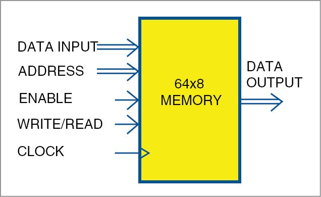
Enable pin triggers the circuit when it is active high, and read operation is performed when read/write pin is high, while write operation is performed when read/write pin is active low.
Software
Verilog has been used for register-transfer logic coding and verification. The bottom-up design has been followed in this project to facilitate easy debugging of various modules. ModelSim is an easy-to-use yet versatile simulator from Mentor Graphics. It supports behavioural, register-transfer- and gate-level modelling.
To start memory (64-bit) design simulation, install ModelSim V 10.4a on a Windows PC and follow the steps mentioned below:
1. Start ModelSim from the desktop; you will see ModelSim10.4a dialogue window
2. Create a project by clicking Jump Start on Welcome screen
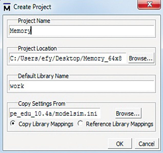
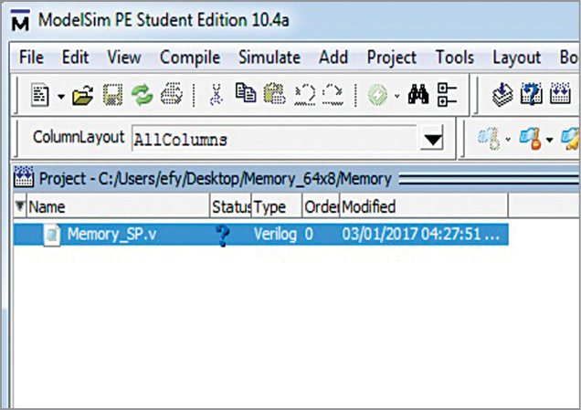
3. Create Project window pops up (Fig. 2). Select a suitable name for your project. Set project location and leave the rest as default, and click OK
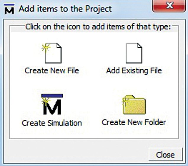
4. Add items to Project window pops up (Fig. 3). Select Create New File option
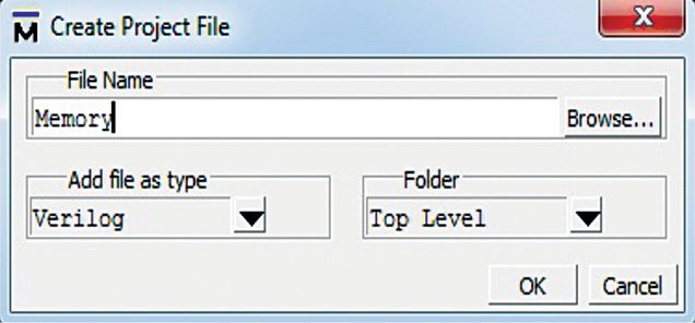
5. Create Project File window pops up. Give an appropriate file name (say, Memory_SP.v) for the file you want to add, and choose Verilog as Add file as type and Top Level as Folder (Fig. 4)
6. On the workspace section of the main window (Fig. 5), double-click on the file you have just created (Memory_SP.v in this case)
7. Type your Verilog code (Memory_SP.v) in the new window. Since 64-bit x 8-bit memory is considered here, 64-bit address is considered, and the main goal is to input 8-bit data that should be written in this address location. Note that these inputs are arbitrary, and you can enter any 8-bit data
8. Save your code from File menu
Note: Generally, memory internal architecture design may contain D-flip-flop, mux, basic cell, 8-bit word, core and so-on.
Compiling/debugging Project Files
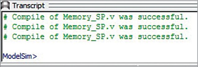
1. Select Compile→Compile All options
2. Compilation result is shown on the main window. If you get ‘Compile of memory-SP.V was successful’ message, it means there are no errors in the project (Fig. 6)
Simulating Memory 64-bit×8-bit Design
1. Click on Library menu from the main window and then click on plus (+) sign next to the work library. You would see Memory_SP that you have just compiled (Fig. 7)
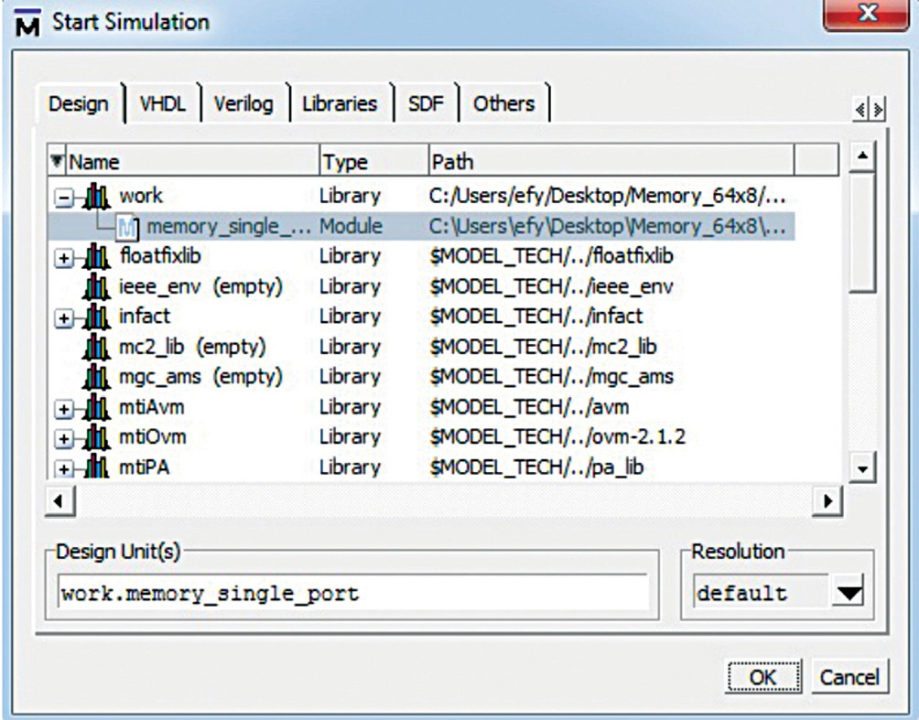
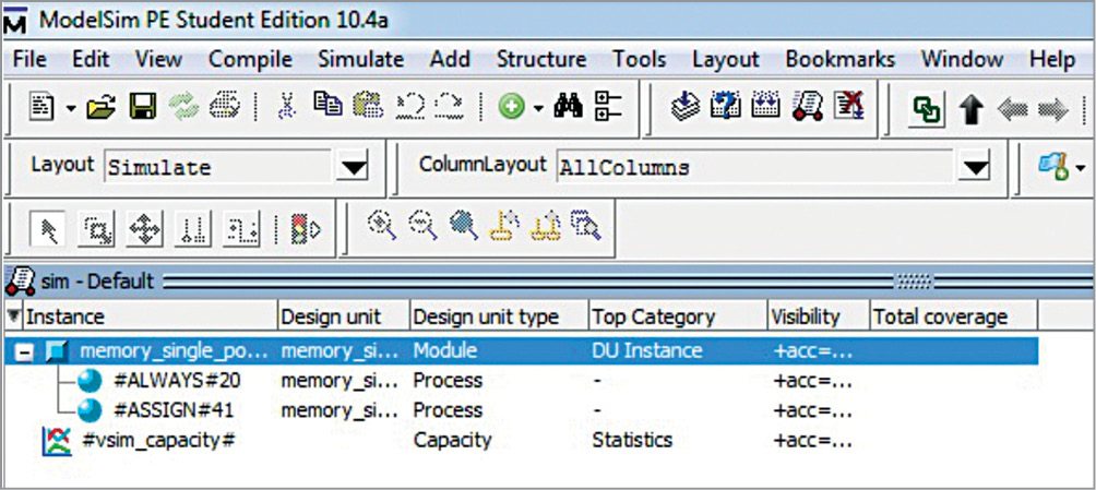
2. In the work library, select as shown in Fig. 7 and click OK. This will open sim-Default window, as shown in Fig. 8
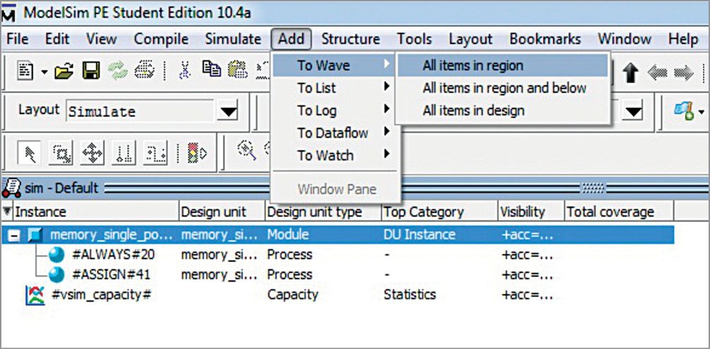
3. Go to Add→To Wave→All items in design options (Fig. 9)
4. Select the signals you want to monitor for simulation purposes. Select these, as shown in Fig. 10
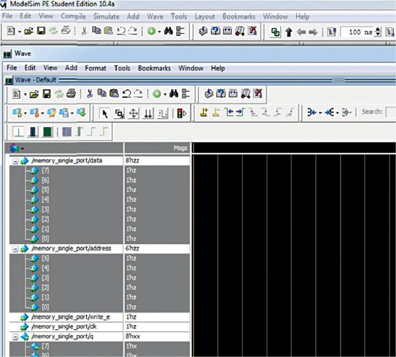
5. Selected signals are used to verify data-write operations in the memory. Simulate your design by clicking Run from Simulate menu bar, as shown in Fig. 11
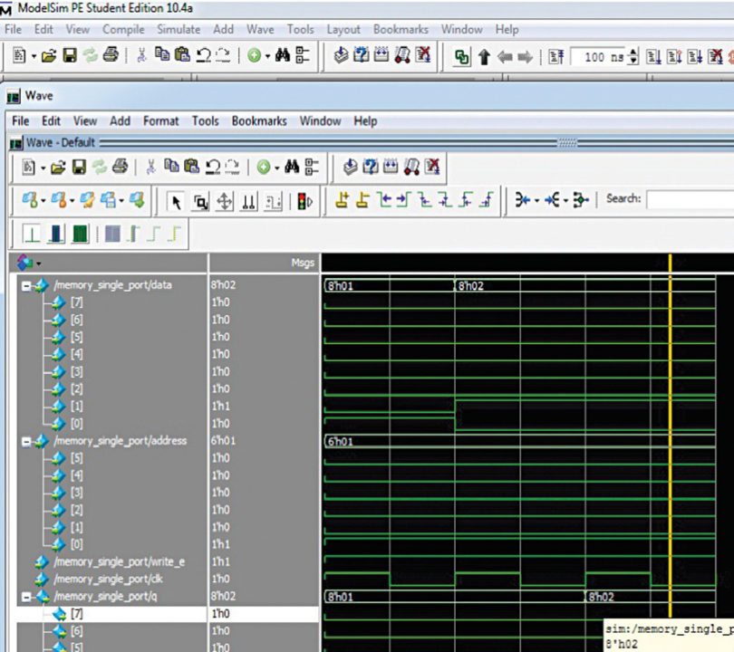
Here, to validate the memory implementation, fill the memory at selected address location between 0 and 63. Perform a random data write operation. Enable and read the data from that particular address location.
Download source code
For reading more exciting software projects: click here
Arnav Bansal is an electronics hobbyist who loves to tinker with circuit designs
