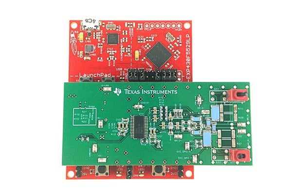
The scale design provides accurate weight measurements, essential in pharmaceuticals, research, and manufacturing, ensuring consistent, reliable results for critical applications.

High-resolution, low-drift, precision weigh-scales are indispensable tools in various industries where accuracy and reliability in weight measurement are paramount. These scales are designed to provide highly accurate readings with minimal deviation over time, making them essential for applications such as pharmaceuticals, laboratory research, jewellery making, and quality control in manufacturing. Their ability to detect minute weight changes is critical in ensuring product consistency, adhering to regulatory standards, and supporting cost-efficient operations. Whether for safety-critical formulations in the chemical industry or precision tasks in scientific research, these scales play a vital role in maintaining the highest standards of measurement accuracy.
The high-resolution, low-drift, precision weight-scale reference design with AC bridge excitation, TIPD188 from Texas Instruments (TI), helps simplify the design process. The reference design for a precision weigh-scale excels by delivering more than 50,000 noise-free resolution counts across a broad temperature spectrum. The design nearly eradicates offset and offset drift errors using an ac-excited, radiometrically measured resistor bridge. Central to this design is the utilisation of the high-resolution ADS1262 delta-sigma ADC, which enhances its measurement accuracy and reliability.
This design finds its applications in diverse fields, including as a CT detector module, in the motor control systems of mobile robots, and in benchtop Near Infrared (NIR) spectrometers. It is also employed in PET demodulator modules, weight scales, and dynamic and static X-ray detectors. Each application benefits from the technology’s precision and reliability, showcasing its versatility in different areas.
This robust circuit reference design comes packed with features that set it apart. The design operates efficiently across a wide temperature range, from -40 ᵒC to +125 ᵒC, with less than 1 μV total error. It includes a 5V ADC supply and bridge excitation voltage, with a bridge output ranging from 0 V to 10 mV. The comprehensive nature of this design is evident in its detailed inclusion of theory, complete error analysis, carefully selected components, simulation, and PCB design. The measured data correlates seamlessly with the theoretical and simulated expectations, demonstrating the design’s effectiveness and reliability.
For this design, the ADS1262, a 32-bit delta-sigma ADC, was selected for its low-noise attributes and integrated Programmable Gain Amplifier (PGA), making it suitable for high-end weight-scale applications. The ADS1262’s PGA can amplify signals up to 32 V/V, and for optimal noise performance, the highest gain setting within the input voltage range is preferred. The TS5A21366, a dual single pole single throw (SPST) 0.75Ω analogue switch, controls the bridge’s excitation voltage polarity for AC excitation, chosen for its voltage compatibility and low on-resistance. The input and reference filters in the design are first-order RC circuits, primarily for anti-aliasing, while the digital filter primarily handles noise rejection.
TI has tested this reference design. It comes with a Bill of Materials (BOM), schematics, etc. You can find additional data about the reference design on the company’s website. To read more about this reference design, click here.


