


If you wish to design a microcontroller-based product from scratch, here is a set of guidelines that will enable you to work from customer requirements, thru defining specifications, designing hardware, setting up a workbench with an Integrated Development Environment and eventually realizing a product that meets customer requirements.
To illustrate the process, I have chosen a working product: “Talking Book” designed specifically for visually challenged children.
The design process is outlined below.

Step 1: Initiating Product Development
- Customer requirements
- Product specifications
- Make a block diagram of the product
- Identify components including microcontroller
- Select components
- Find voltage and current requirements
- Work out schematic
Step 2: Establishing Development Environment
- Identify Integrated Development environment
- Select a programmer/debugger
- Install IDE
- Install compiler
Step 3: Understanding and Initializing Hardware Components
- I/O Ports
- Serial Ports
- interrupts
- MP3 Device
Step 4: Product operation flowcharts
- Data File Organisation
- Navigation flowchart
- Interrupt Flowchart
Step 5: Product testing
- Hardware testing
- Functional testing
Let us start the process.
Step 1: Initiating Product Development
Step 1.1: Customer requirements
A customer requires a learning aid for visually challenged children. Customer says:
I want to help visually challenged children in their studies, so I want a gadget that will speak to children like a teacher and thus teach various subjects to children.
The gadget should have these features:
- Every child will be given one device
- It should be hand-held, light weight, battery powered.
- It should be very easy for the child to operate it so that he/she gets a smooth learning experience.
- He/she should be able to select subject, lesson and any part of selected lesson with ease, using keys.
- Child should be comfortable with the accent of what he/she hears.
- Course material should be in an easily removable memory device to facilitate replacement.
- When child moves to the higher class, another memory device with new contents will replace the current memory device.
Step 1.2: Product specifications
Let us start translating the customer requirements into a device structure:
- The Talking Book is a small handheld instrument powered by a battery.
- Since it is operated by a visually challenged child, it should have tactile keys for accessing content.
- It should have as few keys as possible, so the child is comfortable using it.
- Navigation thru the content of the book should be user-friendly. This requires a thoughtfully developed navigation flowchart.
- It is equipped with memory in which the book is stored.
- Since it is designed primarily for visually challenged children, it does not have a display.
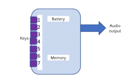
Step 1.3: Make a block diagram of the product
The preliminary translation of user requirement into specifications produces a basic device structure as shown in Fig.1.
Now let us analyse the requirement in more detail.
Step 1.4: Identify components including microcontroller
The book is stored in a removable memory device, true, but in which form?
Text or Audio?
- If we use text form, we will need a text to speech converter [TTS Converter].
- If we use audio form, we will need something like an MP3 player.
- The Customer requirement says, at #5: Child should be comfortable with the accent of what he/she hears.
- If we use TTS converter then ‘accent’ may be an issue that would violate this condition.
- If we use audio files, we can have the content recorded by someone with whose accent the child may be comfortable.
- Hence we decide to store the content in ‘AUDIO’ form with mp3 format. We will use mp3 player.
- Our conclusion is: The audio files are stored in a SD Card and in mp3 format and use readily available mp3 player.
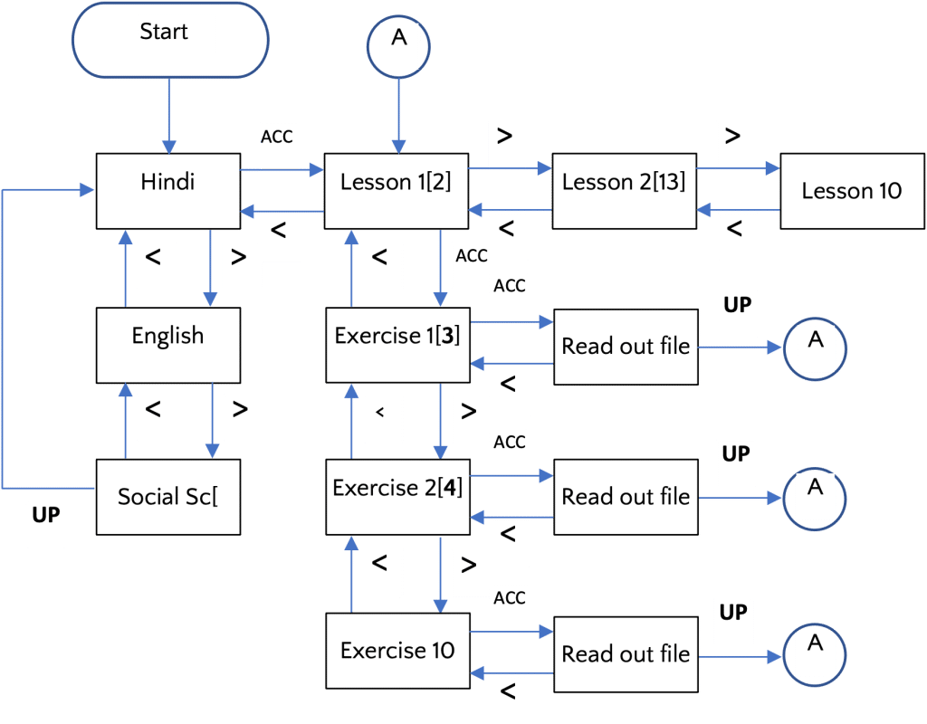
The next issue is the number of keys and their functions. This calls for a decision about file organization and the related matter of user friendly ‘navigation process’.
- I have chosen to have three subjects in my talking book, namely Hindi, English and Social Science. One may choose any other set of subjects, the process as described below will remain the same.
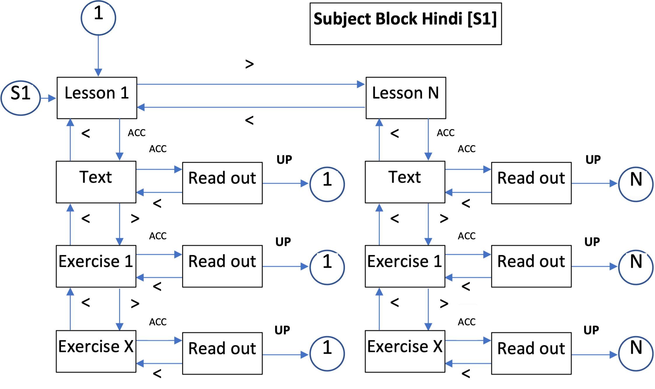
- Each of this subject has a number of lessons and each lesson has ‘Text’ as well as a section of ‘Exercises’.
- Child should be first able to select the subject, then he/she should be able to select either ‘Text’ or Exercises. If he/she selects ‘Exercises’ then he/she should be able to go to any exercise of his/her choice.
- Child should be able to go to a different subject or different Exercise or to Text from the current location.
- The flow chart given below facilitates this operation.
- It uses four keys for navigation, namely, Next[>], Previous[<], Accept[ACC] and UP.
- Initial location on power up/reset is Subject ‘Hindi’, the title.
- User hears the words “Subject Hindi” on power up/reset.
- ‘>’ is used for going to next choice, ‘<’ is used for going to previous choice, ‘ACC’ is used for choosing currently offered location and ‘UP’ takes the child to the top of the Subject.
- If already at the top of the Subject then ‘UP’ takes the child to the previous Subject.
- In this way child can reach any part of the book with ease.
- Every time child reaches a location its title is read out so that child can decide whether to accept or skip forward or backwards.
- Thus we see that four keys are required for navigation. We need two keys for Volume control, VOL+ and VOL-.
- One key is required for PAUSE/PLAY. In this way the total number of keys is 4+2+1=7.
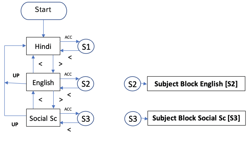
Navigation Flow Chart for Audio Book
Step 1.5: Select components
Step 1.5.1:
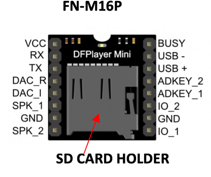
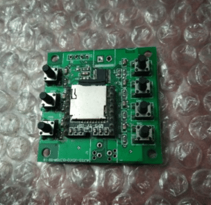
Selecting MP3 Player Now we will look for an MP3 player. Such players are readily available and a google search shows that FN-M16P to be most quoted MP3 player. Let us take a look at it. It has a built in SD Card interface complete with a SD Card holder, Earphone/Audio Amplifier interface, it has serial communication interface for interacting with a microcontroller This is all we need. Let us take a look at its features:
- Supports MP3 and WAV decoding.
- Supports FAT16 and FAT32 file system.
- UART RS232 serial control mode.
- Supports maximum 32GB micro SD card and 32GB USB flash drive.
- Supports maximum 3000 audio files under the root directory of the storage device.
- Supports maximum 99 folders, and each folder can stores 255 audio files.
- Built-in a 3 watts amplifier that can direct drive a 3 watts speaker.
- 30 levels adjustable volume, and 6 levels adjustable EQ.
Step 1.5.2:
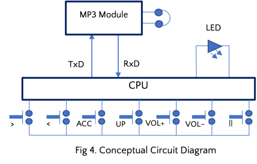
Selecting Microcontroller Based on our analysis, we arrive at a Conceptual Circuit Diagram shown in Fig 4. LED as shown in the diagram is for testing purpose only. Now we need to select a suitable microcontroller. Our analysis as illustrated in Fig 4 tells us that we need SEVEN I/O pins for switches, ONE for LED and TWO pins for serial communication. Apart from this, there will be TWO pins for power, ONE pin for reset and programming pins that depend on the Microcontroller we eventually select. This comes to 7+1+2+2+1+Prog pins = 13+Prog pins.
The requirement is not critical, almost any processor will serve the purpose, but we need to select the one that comes closest to it. Take a look at ST Microelectronics portfolio. You will find a device closest to our requirements, in the STM8S series, a device STM8S003 which has 20 pins, two pins for serial communication, remaining 14 port pins can be I/O pins, but we use only eight, and it needs only ONE pin for programming/debugging. Thus, it meets our bill and leaves scope for any application extension.
Step 1.5.3:
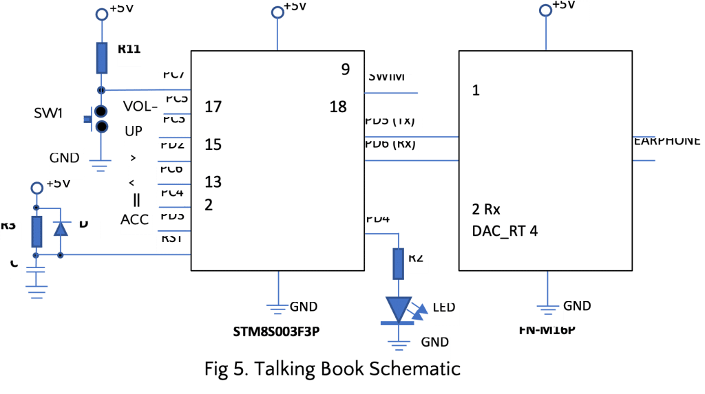
Selecting C, D, LED, R1, R2, R3 [Refer to Fig 5]
R1=10kOhm Selecting LED: Visit https://www.vishay.com/leds/leds-0603/
Part No: TLMS SMD0603
Color: Red/Wavelength: 628nm/Current: If=2mA/Voltage: Vf=1.8V@2mA
Calculate R2: R2=[V5-Vf/If=[5-1.8]/2 kOhm = 1.6kOhm Refer to STM8S003F3 STM8S003K3-DM00024550 and locate Page 75: You will see “9.3.7 Reset pin characteristics” Check: tINFP(NRST) [NRST Input not filtered pulse]: 500ns VIL(NRST) NRST input low level voltage = 0.3 x VDD = 1.5V It also says that C>=10nF, T>500ns
1.5 = 5[1 – e(T/R3.C))]
R3 = 1kOhm, C=22nf
With this selection we get T=22µs
Our hardware picture is complete as shown in Fig 5. For simplicity of drawing only ONE switch is shown connected, namely SW1[VOL+]. Remaining SIX switches are similarly connected as specified in Table 1.
| Switch | SW1 | SW2 | SW3 | SW4 | SW5 | SW6 | SW7 |
| Name | VOL+ | VOL- | UP | > | < | || | ACC |
| Port | PC7 | PC5 | PC3 | PD2 | PC6 | PC4 | PD3 |
| Port Pin | 17 | 15 | 13 | 19 | 16 | 14 | 20 |
Step 1.6:
Find voltage and current requirements
MP3 Player FM-M16P
Working Voltage DC3.3~5.0V; Typical: DC4.2V
Rated Current <15mA
Microcontroller STM8S003F3P
Working Voltage: 2.95V to 5.5V
Rated Current: 4.5mA max at 16MHz clock
Step 1.7:
Work out schematic
Step 2: Establishing Development Environment
Step 2.1: Identify Integrated Development environment
How do you program a microcontroller, how do you know the program is working the way it should, how do you correct it if it is stuck somewhere, may be in an infinite loop; in fact, there may be an impossible situation in which your program is stuck, something beyond your imagination! You need a way to stop running of the program at selected point, you need to see whether variables are taking right values or not.
So, you need a friendly environment to write a program, to compile it, to transfer it to the microcontroller, to link various program files that make up the project, to debug it to remove all sorts of possible errors. Such an environment is called Integrated Development Environment. For our microcontroller, the STM8S series, there is an environment called “ST Visual Develop” or simply STVD.
You also need a means for connecting your product board to your computer. You need a device called ‘Programmer/Debugger’.
Step 2.2: Select a programmer/debugger
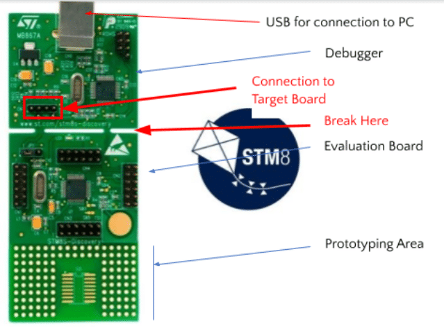
If you visit https://www.st.com/content/st_com/en/products/evaluation-tools/product-evaluation-tools/mcu-mpu-eval-tools/stm8-mcu-eval-tools/stm8-mcu-eval-boards/stm8s-discovery.html you will find debugger suitable for STM8S series of devices. There are THREE distinct parts of this device: 1. Debugger, 2. Evaluation Board, 3. Prototyping area. You may develop software of your product on the evaluation board. In case you need to add some components for realising your project, there is a prototyping area that you can populate.
Once you have your own product board, you may break at the line shown above and use only the “Debugger” and connect it to your board using pins shown in a RED rectangle.
There are only FOUR pins: Two pins carry power-VDD and GND, ONE pin for SWIM [Single Wire Interface Module- the actual debugging control], and ONE for RESET input. You need to have provision on circuit board of your product for connection to these four pins.
Step 2.3: Install IDE
Go to this link to read about this IDE called STVD-STM8S: https://www.st.com/en/development-tools/stvd-stm8.html Or, you may go directly to this link and then download the IDE. This involves registering. https://www.st.com/en/development-tools/stvd-stm8.html#get-software Having done that you will also need to download a compiler, also free, to complete the package. Compiler can be downloaded from the Cosmic site. You will be asked to register, so, register and download for free: https://cosmicsoftware.com/download.php#stm8_free
You should download STVD-STM8S and the ‘C compiler from Cosmic. Then you will see these two zip files: en.stvd-stm8 and cxstm8_FSE_stm32_32K. Unzip these files and you will see two folders in the folder program files (x86): STMicroelectronics COSMIC. Follow this: STMicroelectronics>st_toolset>STVD>stvdebug.
Thus you reach the IDE application. Double click on it and it will open on your desktop. We will see how to use it later. You can download it even if you don’t have the hardware.
Step 2.4: Install compiler
You have already unzipped COSMIC and so you have the compiler in this location:
Verify this: C:\program files(x86)\COSMIC\CXSTM8_EVAL\Hstm8.
So the compiler is with you but it is not yet a part of IDE. So let us complete the process of installing it in IDE.
You have already opened the IDE on the desktop.
On the top row you will see ‘File’ in the menu. Click on File then on ‘New Workspace’. A new window will open where you are prompted to choose an option; choose ‘Create workspace and project’. You will be prompted to enter a name for workspace. Let us call it Jan22.
Location of workspace is visible; C:\Program Files(x86)\STMicroelectronics\stvd.
Click OK. Another dialog box will appear. Here you will be asked to write Project File name. Let us enter TalkingBook; [Enter any name of your choice]. Its location will be shown in the next line.
Workspace and Project File will be in the same location by default; you may change if you wish.
On the same pop up window select the “Toolchain” that is, the compiler. You get several options in the dropdown menu. One of the options is “STM8 COSMIC”. Select it.
Then you will be shown some “Toolchain root”. Here you enter the complete path of Cosmic compiler. In my case it is: C:\program files(x86)\COSMIC\CXSTM8_EVAL.
With this operation you have installed the compiler in the IDE.
Press Ok and another window will pop-up, called “MCU Selection”. Select STM8S003K3 from the drop down menu and press Select and press Ok.
Recap:
- Workspace name: Jan22; Project name: TalkingBook.
- Workspace and Project file location: C:\Program Files(x86)\STMicroelectronics\stvd
- Compiler [Toolchain] location: C:\program files(x86)\COSMIC\CXSTM8_EVAL
Now you are ready for developing programs for embedded design.
Step 3: Understanding and Initializing Hardware Components
Microcontrollers offer a very wide range of peripherals like I/Os, ADC, DAC, I2C, SPI, USB, UART, USART, Temperature Sensors, etc. Each peripheral is loaded with a variety of interesting capabilities. We need to understand these peripherals thoroughly and then apply their appropriate capabilities to our benefit.
All peripherals possess an ability to interrupt the operation under a variety of conditions. So we also need to clearly understand interrupt capabilities of peripherals deployed in our project.
In the present instance we are going to need only two peripherals – I/Os and UART, with/without Interrupt capability.
Step 3.1: I/O Ports
Every bit of a port is connected to a device pin. Content of the port bit appears as voltage level on device pin if the port pin is in output mode.
Voltage level, logic High or Low, of a physical port pin appears as logic 1 or 0 bit the corresponding port pin.
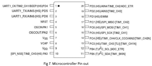
For example, bits 4 and 5 of Port D register, denoted by PD4 and PD5 respectively are linked to CPU pins 1 and 2 as shown in Fig 7. If PD4 is defined as an output port and PD5 as input port then what will happen? If you write 1 or 0 to port D output register it will appear as logic level 1 or logic 0 at CPU pin 1. If you apply logic 0 or logic 1 to pin 2 of the CPU then bit 5 of Port D input register will become 0 or 1 respectively.
Before you can use a port, each pin of the port needs to be initialised, that is, behaviour of each pin needs to be defined.
Following registers define behaviour of pins of registers. In the description below, ‘x’ stands for any port from Port A to Port F.
Px_DDR: Portx Data Direction Register
Px_ODR: Portx Output Data Register
Px_IDR: Portx Input Data Register
Px_CR1: Portx Data Control Register -1
Px_CR2: Portx Data Control Register -2
Portx Data Direction Register
| bit7 | Bit6 | Bit5 | Bit4 | Bit3 | Bit2 | Bit1 | Bit0 |
Writing a ‘0’ to a bit turns that bit in to Input Mode
Writing a ‘1’ to a bit turns that bit in to Output Mode
For example, if Port D Data Direction Register is assigned values as shown, then
| 1 | 0 | 1 | 1 | 0 | 0 | 0 | 1 |
Port D pins 7, 5, 4 and 0 become Outputs and pins 6, 3, 2 and 1 become Inputs.
To do this, we write
PD_DDR= 0b10110001 or in Hex format we write PA_DDR = 0xB1.
So the first step is to define port pins as inputs and outputs, then use the port.
More in Input Mode
When we configure a pin as input, we also have to specify whether it will generate an interrupt, whether it is floating or it has a pull-up resistor.
If a bit in Px_CR1 register is 1 then the input will have a built-in pull-up otherwise it will be a floating input.
If a bit in Px_CR2 register is 1 then the input will have interrupt capability i.e., when input changes in a specified way, it will cause an interrupt. That ‘specific way’ is defined in another register, EXTI_CR1.
More in Output Mode
When we configure a pin as an output, we have to define if it is open drain o/p, push-pull o/p, or whether it has a fast operation mode.
If a bit in Px_CR1 register is 1, then the output is push-pull type else it is Open Drain type.
If a bit in Px_CR2 register is 1, then the output is in fast mode.
Let us take an example, refer to Fig 5.
Port C pins PC3 thru PC7 read switches. So these pins should be in the Input Mode. PC0, PC1 and PC2 are not available to user. Pull up is not required on the switch inputs since we have connected an external pull up resistance. Suppose we want the switches to create interrupts. Then the PC3 to PC7 bits in PC_CR2 should be set to ONE.
| 1 | 1 | 1 | 1 | 1 | 0 | 0 | 0 |
PC_CR2 =
If you do not want to affect Bit0,1 and 2 then you can write this way:
PC_DDR |=0xF8 in hex format. Symbol “|” means logical OR operation.
x x x x x x x x
OR 1 1 1 1 1 0 0 0
—————-
1 1 1 1 1 x x x
Now let us look at PORT D. Refer to Fig 5. Pin 1 is connected to bit 4 of PORT D and it drives a LED. So PD4 should be in O/P mode.
PD2 [Pin 19] and PD3[Pin 20] are in I/P mode as they are driven by switches.
PD5 is Tx, so it is O/P pin and PD6 is Rx, so it is a I/P pin.
| x | 0 | 1 | 1 | 0 | 0 | x | x |
PD_DDR=
We may write
PD_DDR & = 0xB3; [=10110011], this will clear bits 2,3 and 6 as required
PD_DDR |= 0x30; [=00110000], this will set bits 4 and 5 to ‘1’ as required.
This process will not affect any other bit.
We must make bits 4 and 5 as push-pull. Look at Pin 1 that feeds one LED and is controlled by PD4. If PD4 is configured as ‘Open Drain’ then LED can not be driven at all, since there will be no path between 5V supply and LED. Thus PD4 has to be in push-pull mode. We will make PD5 also push-pull.
PD_CR1 |=0x30; this will set bits 4 and 5 as ‘1’ without affecting any other bit.
Step 3.2: Serial Ports
Our CPU supports UART1 in the 20-pin version. In this series we also have UART2, UART3 and UART4 in devices having more pins. We need only one UART hence present form is acceptable.
As seen above, PD5 [Tx] is on pin 2 and PD6 [Rx] is at pin 3.
UART registers are described at page363 under Section 22.7.
Let us first define characteristics of UART [Universal Asynchronous Receiver Transmitter].
It has to communicate with MP3 Module which has a fixed set of requirements which our UART must match.
Baud Rate=9600, Start bit One, Stop bit One, data length 8 bits.
Also note that our CPU has an internal RC oscillator running at 16MHz; we are going to use it. Equipped with this data we proceed to configure our UART.
Let us start with baud Rate. Our clock is 16MHz and Baud rate is 9600. There is a divisor register which should contain 16000000/9600 = 1667 which expressed in hex is 0x0683. We write this value to the two part divisor register. [Page 365,366]
USART_BRR1=0x68
USART_BRR2=0x03. Look at the strange way in which data is broken and written. First[0] and last[3] hex nibbles are combined and written to BRR2 whereas two middle nibbles[68] are written in BRR1.
USART1_CR1 & = 0xCE; it clears bits 4 and 5 without affecting other bits. Bit 5 is UARTD i.e., Disable UART. Making it ZERO, enables UART. Bit 4 is M, the word length. When this bit is made ZERO, it configures serial data format thus: 1 Start bit, 8 Data bits, n Stop bit (n depending on STOP[1:0] bits in the UART_CR3 register)
USART1_CR2 |=0x2C; 0010 1100 This will set bits 2[REN=Receiver Enable], 3[TEN=Transmitter Enable] and 5[Receiver Interrupt Enable] without affecting other bits. [Page 367]
CLK_ICKCR | = 0x01; this sets Bit 0[HSIEN=High Speed Internal Oscillator Enable] [Page 90]
CLK_ECKCR &= 0xFE; it clears Bit 0[HSEEN =High Speed External Crystal Oscillator Enable=0]
CLK_CKDIVR = 0; Clears bits 0,1 and 2[CPUDIV=000 Sets fsys=Fmaster; so both oscillators are 16MHz]; Clears bits 3 and 4[HSIDIV=00: High speed internal clock prescaling factor is 1 so fHSI= fHSI RC output [Page 94]
CLK_PCKENR1 |= 0x08; Sets Bit 3 without affecting other bits. This connects system clock to UART.
This completes initialisation of UART.
Step 3.3: Interrupts
Switches are connected to Port C pins PC3, 4,5,6 and PC7 as well as Port D pins 2 and 3. We will use I/P pin interrupt in such a way that key bouncing can be eliminated.
We will also use Receive interrupt in UART operation.
Step 3.3.1: I/O interrupt
We have seen earlier that Px_CR2 can be used for configuring I/P pin interrupt.
PC_CR2 |= 0b1111 1000 = 0xF8
PD_CR2 |= 0b0000 1100 = 0x0C
Further we want the interrupt to occur when input voltage level falls and stays low. This condition is met when we initialise External interrupt control register 1 (EXTI_CR1)[Page 70].
EXTI_CR1 &= 0b0000 1111 = 0x0F.
Step 3.3.2: UART Interrupt
USART1_CR2 |= 0b0010 0000 = 0x20; this enables Receiver interrupt.
Status register (UART_SR) bit 5 [RXNE] is set when received data is ready to be read.
Reading UART_SR clears RXNE bit.
Step 3.4: MP3 Device
We have seen relevant hardware details of MP3 module. Now let us see the role of serial communication. When we send an appropriate command string over serial communication link, UART, then one of the five functions is activated:
Accessing desired file in the memory space of SD Card
- Play
- Pause
- Increase volume
- decrease volume
Format of Command String: It consists of TEN bytes. Highlighted bytes stated in hex format are fixed irrespective of command.
| 7E | FF | 06 | Command | 01 | P_MSB | P_LSB | C_MSB | C_LSB | EF |
P_MSB/P_LSB stand for MSB and LSB of parameter. C_MSB/C_LSB stand for MSB and LSB of checksum. Let us see the commands that perform the FIVE functions mentioned above.
| Function Code | Function | Remark |
| 0x03 | Specify a track [1 to 3000] | Initialise to 1 |
| 0x04 | Increase volume | |
| 0x05 | Decrease volume | |
| 0x0D | Play | Initialise to Play |
| 0x0E | Pause | |
| 0x06 | Specify volume [0…30] | Initialise to 30 |
| 0x09 | Specify playback of a device [0:USB; 1:SD Card | Initialise to 1[SD Card] |
What is a Parameter?
When you give command 0x03, Track Number is the Parameter. It ranges from 1 to 3000.
When you give command 0x06, Volume is the Parameter. It ranges from 0 to 30.
When you give command 0x09, Memory Device Code is the Parameter. It is either 0 or 1.
Remaining commands do not have Parameter. You may write ‘0’ for it.
Checksum Calculation
Add six bytes starting from the second byte from left then take its complement. For example, if the string is: 7E FF 06 0D 00 00 00 xx xx EF then do this: 0xFF+0x06+0x0D+0x00+0x00+0x00= 0x0112
Take 2’s complement of 112 which is 0xFEEE
So we can replace xx xx of the string by FE EE.
The string then becomes 7E FF 06 0D 00 00 00 FE EE EF.
In this way we see that all specified functions can be implemented using serial communication.
Step 4: Product operation flowcharts
There are two main flowcharts: Main flowchart and Interrupt flowchart. To understand these flowcharts, one has to be very clear about data file organisation.
Step 4.1: Data File Organisation
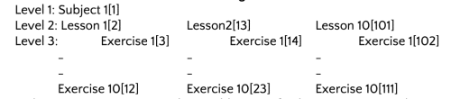
Files are numbered because a file is accessed by its number. Here we see how audio files are numbered. Navigation leads us to desired file number. So organisation of file decides flowchart of navigation.
We have decided to cover only THREE SUBJECTS: Hindi, English and Social Science. But the treatment given here can be easily generalised.
The whole set of files is divided in to THREE LEVELS:
Level 1: Subject Name [There are3 subjects]
Level 2: Subject name, lesson number and lesson title. [There are 10 lessons]
Level 3: Subject name, lesson number and lesson title. Exercise number and exercise title. [There are 10 exercises in each lesson]
Remember, these are Audio Files. When these files are played, user will hear the content.
We have three files at level 1, thirty files at level 2 and three hundred files at level 3. Thus there are a total of 333 files.
Initially user is at level 1, file number 1. If user selects Subject 1 on hearing “Subject one Hindi” then system flow goes to level 2 and announces, “Subject one Hindi lesson one”.
This file is numbered 2. If user selects lesson 1 then flow control goes to Level 3 and Exercise 1 and announces, “Subject one Hindi lesson one exercise one” as the flow moves to file number 3.
Arrangement of Audio Files
Step 4.2: Navigation Flowchart
Program flow for calculating FILE NUMBER on every key closure.
Note
What is true [with respect to flow and file number] with ‘Hindi’ is also true with English and Social Science. Whatever is true with Lesson 1 is also true with every other lesson.
File number is shown in the parenthesis.
- Address of Exercise10 of Hindi-Lesson 10 is 111.
- Address of Exercise10 of English-Lesson 10 is 222.
- Address of Exercise10 of Social Science-Lesson 10 is 333.
Audio: File number of the file to be played is updated every time user presses a key and then that file is played.
For example, when Exercise 10 of Hindi Lesson1 is selected it plays file number 12.
Step 4.3: Interrupt Flowchart
1: ACC [Accept] 2: > [Next] 3: < [Previous] 4: Up [Move one level up]
5: Vol+ [Increase Audio Volume] 6: Vol- [Decrease Audio Volume]
7: Play/Pause
We have configured PC3 to PC7 and PD2, PD3 such that if input to corresponding pins falls to zero and stays low then interrupt is generated.
Note: When an interrupt occurs, program branches to a specific address. This address is known as a Vector.
There is one address for interrupts caused by any pin of Port C. How to find out which pin of Port C caused the interrupt. Answer is, read Port C and you will know which pin went low. That is the pin that caused interrupt. Same rule applies to Port D also, in fact it applies to all ports.
Program segment will look like this:
INTERRUPT_HANDLER (EXTI_PORTC_IRQHandler, 5)
{
If(!(PC_IDR & 0x40)) // This checks PC6: 0100 0000
{
Key=5; // VOL- key
PC_CR2 &=0x07; // Clear entire Port C
}
If(!(PC_IDR & 0x08)) // This checks PC3: 0000 1000
{
Key=3; // UP key
PC_CR2 &=0x07; // Clear entire Port C
}
If(!(PC_IDR & 0x80)) // This checks PC7: 1000 0000
{
Key=4; // UP key
PC_CR2 &=0x07; // Clear entire Port C
}
If(!(PC_IDR & 0x20)) // This checks PC5: 0010 0000
{
Key=5; // < key
PC_CR2 &=0x07; // Clear entire Port C
}
If(!(PC_IDR & 0x08)) // This checks PC4: 0001 0000
{
Key=7; // Pause key
PC_CR2 &=0x07; // Clear entire Port C
}
}.
Similarly for Port D interrupts.
When main program finds a non-zero value of variable ‘Key’, it will follow this sequence:
If value of Key is less than 5 then it knows it is a navigation key. It deciphers the meaning and generates appropriate file number, assembles the 10-byte string and sends the string on the serial port whereupon MP3 device starts reading the file that you can hear on the earphones.
If value of Key is more than 4 it deciphers the meaning of the key, assembles the 10- byte string and sends the string on the serial port. Note that in this case it does not affect file number. It either increases/decreases volume of sound or Plays/Pauses audio output.
Thereafter it enables key interrupts.
Step 5: Product testing
With some effort you can use the evaluation board and the code supplied with this article to verify operation of the Talking Book.
You may alternatively use the board of the talking Book and use above program and have a real experience of a talking book.
This device is powered by three rechargeable Ni-MH cells giving a nominal voltage of 3.6V.
Step 5.1: Hardware testing
(a) Make sure that connections are as per the schematic. (b)Power up. (c)Check voltage of VDD with reference to VSS. (d) Check voltages at pins 13,14,15,16,17,19 and 20 with reference to VSS; these voltages should be equal to VDD.
Step 5.2: Functional testing
(a)Create a data file in the SD Card as per Step 4.1 and insert the card in the socket on MP3 Module.
(b) Create Workspace, Project etc on the “stvdebug” IDE and load the three program files.
(c)Select “Debug” tab and then use “Build” tab; you will see:“0 error(s),0 warning(s)”.
(d) Connect hardware.
(e)Use “Debug” tab to transfer program to the microcontroller.
(f) Use “Run” tab. LED should flash.
(g) Use “Stop program” tab.
(h) Use “Restart application” tab so that program goes to starting point and halts.
(i)Set break points on all lines that contain PC_CR2 &=0x07 and PD_CR2 &=0xF9.
(j) Run the program. Press the keys in sequence from 1 to 7. Program will halt every time you press a key. You can check whether key identifier is right.
(k) Remove break points and test the jumps in files as per flowchart by pressing various keys. This will complete the navigation testing part of functionality.
(l) Check control Keys – Vol+, Vol- and Pause/Play.
Having tested ok, rebuild the program using “Release” option from the tab that you used for building for “Debug”. The program is now fir for Production. Disconnect the debugger, power up the device from battery and test the device independent of PC.
Conclusion
The article demonstrates how we start from “Customer Requirements”, translate these requirements to “Technical Specifications”, choose components and design hardware to realize these specifications, develop flow charts to realize functionality, build and test programs using appropriate IDE. In the process we also learn to use IDE and to write ‘C programs.
In passing one may mention that Quality Procedures involve two kinds of tests – Verification and Validation. Verification refers to the process of verifying that product works as per “Specifications” and Validation refers to the process of verifying that product meets “Customer Requirements”. It is of paramount importance that you translate customer requirements into Specifications correctly otherwise all your effort will come to a null.
NOTE: Wherever “Page No” is mentioned, it refers to ST Microelectronics document “STM8S003F3 STM8S003K3-DM00024550”.

I do not know who you are but you have written a beautiful book , It explains something I have been searching for for over 15 years, you see ,I started programing with arduino but never has anyone except you led me down the path of product development using a microcontroller in an understandable way. Now I have a roadmap that can be used to create all kinds of neat stuff that I have dreamed up over the years, yes I can blink leds, put letters and numbers on an 4X16 lcd and even put photos on a tft lcd, make noise and smoke( the blue type) when the power is connected backwards and now have a method to putting an electronic device on the shelves of “amazon” Wow THANK YOU VERY MUCH and please send a copy of this development article to Instructable’s.
Thank you for your valuable feedback.