


Featuring high efficiency, minimal THD, and user-friendly software, the reference design seamlessly addresses unpredictable load challenges.
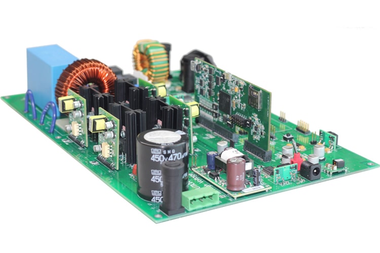
Voltage source inverters (VSIs) are frequently employed in uninterruptible power supplies (UPS) to produce a consistent AC voltage at the output. However, designing control for these inverters can be intricate due to the unpredictable loads that might be linked to the inverter’s output. Addressing these challenges and needs, a reference design of a single-phase inverter has been introduced by Texas Instruments (TI). The reference design utilises a C2000 microcontroller (MCU) to control a single-phase inverter (DC/AC). It offers dual operational modes for the inverter. One is the voltage source mode with an output Inductor-Capacitor (LC) filter, and the other is a grid-connected mode featuring an Inductor-Capacitor-Inductor (LCL) output filter. With its high efficiency, minimal Total Harmonic Distortion (THD), and user-friendly software, this model is particularly appealing for professionals designing inverters for UPS and renewable energy endeavours, including PV inverters, grid storage, and microgrids.
The reference design has an input voltage of 380-DC VIN, with an output of 110V Root Mean Square (RMS) at 60 Hz or 22V RMS. Users can select between 60 Hz or 50 Hz for output, and it offers a maximum output of 600-VA. The device achieves a peak efficiency of 98% and employs a 20-kHz switching mechanism. Regarding harmonic performance, its THD is less than 1% for linear loads and less than 3% for typical non-linear loads when using Sigma-Delta Frequency Modulation (SDFM). With Analog to Digital Converter (ADC), these values are less than 2% for linear loads and less than 4% for typical non-linear loads. The operation of the controller can be selected based on either cold or hot scenarios, meaning it can work on isolated or non-isolated sides.

A standard inverter is made up of a full bridge constructed with four switches. These switches can be controlled using pulse width modulation (PWM). Accompanying this bridge is a filter designed for its high-frequency switching. An inductor-capacitor (LC) output filter is employed for this reference design. To maintain a consistent output voltage from the inverter, current and voltages must be detected. The MCU’s on-chip ADCs provide a rapid and accurate means to sense these signals. The software associated with this reference design is organised into three sequential builds: an open loop, a closed current loop, and a closed voltage loop with an inner current loop. These are further supplemented by various testing options for evaluating the control loop design. This step-by-step approach streamlines both system initiation and the overall design process.
TI has tested this reference design. It comes with a Bill of Materials (BOM), schematics, Gerber file, etc. You can find additional data about the reference design on the company’s website. To read more about this reference design, click here.
