


 A simple explanation for the working of an ideal diode circuit based on P-channel MOSFET and PNP transistor is presented here. The typical voltage required to turn on a diode is forward voltage. An ideal diode should have zero forward voltage but, unfortunately, there is no such thing as an ideal diode.
A real diode has forward voltage drop and reverse leakage current. Even a Schottky diode has a forward voltage drop between 0.2V and 0.4V, which can be significant, especially when used in series with batteries with lower voltages that reduce the efficiency and life of the batteries.
Many diode applications require reverse current blocking, most common applications being battery-operated circuits. Another example of a diode application is reverse voltage or reverse current protection for USB supply as used in Raspberry Pi 3.
Limitations of a practical diode call for the need of a near-ideal diode with as little forward voltage drop as possible. While selecting a practical diode, its forward voltage and reverse leakage current should be as low as possible. Simulation and testing results in this article showcase the working of the typical circuit of an ideal diode or smart diode. Details for designing the circuit are also provided to enable you to easily adapt the circuit to your designs.
Circuit and working
The circuit consists of P-channel enhancement mode MOSFET (Q1), two PNP transistors (Q2A and Q2B) and three resistors (R1, R2 and R3), as shown in Fig. 1.
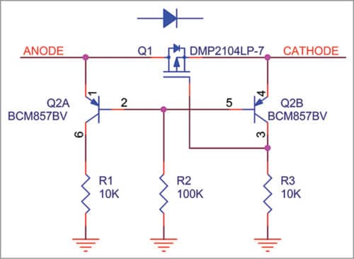
Q1 is the series element, and the two bipolar junction transistors, or BJTs (Q2A and Q2B) are the control elements that turn Q1 on or off. When Q1 is on, it acts as a diode in forward bias condition, and when it is off, it acts as a diode in reverse bias condition.
Source of Q1 is connected to cathode side, and the drain to anode side, to ensure the body of MOSFET is reverse-biased. The gate is controlled by cathode side BJT (Q2B). When Q2B is on, Q1 will be off, and vice-versa.
Both BJTs are designed to work as switches. Emitters of BJTs are connected to anode and cathode sides, and bases are tied together. Base-emitter junctions of the two transistors effectively become OR-ing diodes for voltages at anode and cathode sides. Base-emitter junction of the transistor at the higher voltage side will be forward-biased, while the other will be reverse-biased.
Since BJTs are configured to work as switches, the one with the higher voltage at emitter will be on, thereby forcing the other BJT to be off. This is the simplicity of the circuit. When voltage at cathode side is higher, Q2B will be on and Q1 will be off, making the diode reverse-biased.
Base-emitter voltage drop (VBE) of the transistors needs to be as equal as possible to ensure the circuit reacts to the slightest difference in cathode and anode side voltages. It is highly recommended to use a matched pair PNP transistor for the application.
The circuit in Fig. 1 will take the shape of a current mirror if emitters of both BJTs are shorted. In a current mirror, current through the right-side transistor will depend only on current through the left-side transistor, for a given temperature. However, in this circuit, emitters do not get shorted even when Q1 is on, since Q1 connected in series introduces a voltage drop that depends on the gate to source voltage (VGS) and drain current (ID) of Q1.
That is, with the introduction of Q1, more parameters get introduced. Voltage drop across transistor Q2B is effectively gate-to-source voltage (VGS) of Q1. To keep Q1 in saturation, voltage drop across Q2B needs to be more than the threshold voltage (VT) of Q1.
Another parameter that depends on VGS is current through Q1. Thus, Q2B goes to active region instead of cut-off region with a value of collector current balancing the different parameters. Calculating this collector current is a tedious exercise, as the value varies with applied voltage, resistors, MOSFET parameters, load current and so on. The easiest option is to simulate the circuit.
Simulation
Simulation software is recommended to simulate and analyse the circuit before implementation. Here, we used LT SPICE, a free simulation software. Simulations are performed by applying a triangular wave of amplitude 0V-5V, 1Hz at anode side and fixed 2.5V at cathode side.
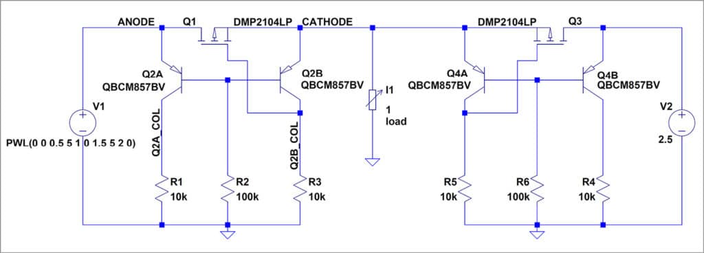
As explained earlier, once MOSFET is connected, waveform at collector of Q2B will get modified depending on load current. To avoid the effect of voltage sources on load current, two ideal diodes (Q1 and Q3) are connected back-to-back with a variable load connected between these diodes, as shown in Fig. 2. Waveforms captured for left-side ideal diode (Q1) are shown in Figs 3 and 4.
Results in Figs 3 and 4 clearly show that voltage across cathode side transistor Q2B depends on load current (IL).
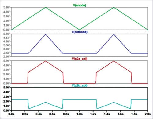
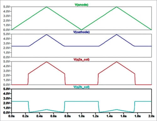
Dependence on VGS may be observed by using a different MOSFET in simulation or by editing SPICE model. There is a small voltage drop on cathode voltage due to resistive voltage drop of MOSFET, which is not quite evident in the waveforms as resistance of the selected MOSFET is quite low.
Download source folder: click here
Design considerations
1. As mentioned earlier, the major parameter to be considered while selecting the BJTs is difference in VBE voltages. Mismatch in VBE voltages of transistors can cause the MOSFET to be undesirably on or off for small differences in voltages on either side.
If voltage difference between anode and cathode sides is large, any suitable transistors can be used. But this may not be the case for majority of the designs calling for the need of matched pair transistors.
2. The next parameter to be considered is saturation current (IC(Sat)). Since saturation current of the transistor is leakage current in the circuit, this should be kept as low as required.
Collector-emitter saturation voltage (VCE(sat)) of the BJT is another parameter to be considered, which will affect the selection of MOSFET. If there is any chance of negative voltage stress on the BJTs, emitter-base breakdown voltage (BVEBO) might also need to be considered.
3. Selection of MOSFET largely depends on application. Major parameters to be considered are drain-source breakdown voltage (BVDSS), static drain-source on-resistance (RDS(ON)), maximum continuous drain current (ID) and gate threshold voltage.
Drain-source voltage should be selected as per maximum possible voltage difference between anode and cathode sides. On-state resistance of MOSFET will cause voltage drop across the FET, which would become the effective forward drop of the diode.
RDS(ON) shall be kept as low as possible to keep voltage drop at minimum. Gate threshold voltage should be selected so that absolute value of minimum VGS(th) is more than VCE(Sat) of transistor and maximum is less than minimum voltage applied to the MOSFET (VCE(Sat)<|VGS(th)|< VIN(Min))).
4. Design of the circuit is quite simple, as it only requires the use of both transistors as switches. Collector resistances and base resistance need to be calculated properly to ensure the transistor will be in saturation mode for the expected voltage range of operation, yet saturation current should be as low as acceptable.
Avinash Manu Aravindan is a systems design engineer with over nine years of industry experience. His interests include embedded systems design, high-speed systems design, mixed-signal systems design and statistical signal processing

Nice explanation
I don’t see it mentioned in the article, but this circuit is good for reverse voltage applications below 5V (in magnitude) or so. Above that, the emitters break down.