
During soldering, lead fumes are generated, which are toxic. The flux used for soldering also emits fumes, which again are highly toxic if inhaled in excess. So it is always better to remove these toxic fumes from the working area. The circuit described here removes these toxic fumes from the area automatically, when required, using a small exhaust fan.
Must read: Choosing the Best Soldering-De-soldering Workstation.
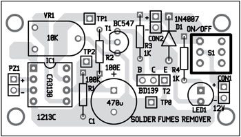
Solder Fumes RemoverCircuit and working
The circuit diagram of a solder fumes remover is shown in Fig. 1. The circuit is built around the popular op-amp CA3130 (IC1), transistors BC547 and BD139 (T1 and T2, respectively), a 12V DC small exhaust fan and some easily-available components.


CA3130 is an excellent op-amp that requires very low input current. It is a 15MHz BiMOS IC with MOSFET inputs and a bipolar output. MOSFET transistors present in its inputs provide very high input impedance. The input current can be as low as 5 pA. Presence of these PMOS transistors results in a common-mode input voltage down to 0.5 volts below the negative rail. The internal bias of the IC at 5 pA is sufficient for its working, thus external biasing is not required in this case.
A heat sink with piezoelectric element PZ1 attached to it is placed on the soldering stand to sense heat from the soldering iron tip. PZ1 is directly connected to the inputs of IC1 as shown in Fig. 1. It generates a small voltage due to its piezoelectric property when stressed by heat.
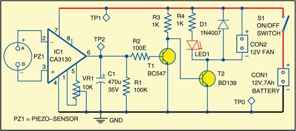
When you are soldering a joint, the soldering iron is away from PZ1. Thus output of IC1 is low, since its inputs are almost balanced. So transistor T1 does not conduct, but transistor T2 conducts and switches on the exhaust fan to remove the fumes generated during soldering.
After soldering, when you keep the soldering iron back into the soldering stand, the heat from the soldering tip creates stress on the piezoelectric element. This generates around one volt, which upsets the input balance and the output turns high. So transistor T1 conducts and T2 stops conducting, and the fan also stops.
Preset VR1 is used for the offset null adjustment of IC1. Capacitor C1 is added as a buffer so that T1 remains on even if the output of IC1 turns low momentarily. Capacitor C1 discharges through resistor R1 when the output of IC1 goes low.
Working of the circuit is simple. During soldering, the exhaust fan runs, but it stops when you keep the soldering iron back on the soldering stand.
Download PCB and component layout PDFs: click here
Testing Solder Fumes Remover
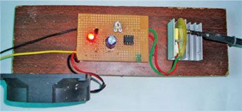
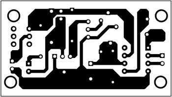
An actual-size, single-side PCB for the solder fumes remover is shown in Fig. 3 and its component layout in Fig. 4. After assembling the circuit on PCB, enclose it in a suitable plastic case.
The fan should be fixed so as to work like an exhaust fan. Connect the piezoelectric element to the circuit using thin wires and glue it on the heat sink. Heat sink with the piezoelectric element should be fixed on the soldering iron stand such that the tip of the iron almost touches the heat sink assembly.
Verify the correct power supply for the circuit at TP1 with respect to TP0. Verify the logic level at TP2 corresponding to the position of the soldering iron.
Also, check 6 DIYs for a Supersonic Soldering Station.
The author is an associate professor at Government College for Women, Thiruvanthapuram, Kerala. He is a regular contributor to EFY